当前位置:
X-MOL 学术
›
Adv. Healthcare Mater.
›
论文详情
Our official English website, www.x-mol.net, welcomes your
feedback! (Note: you will need to create a separate account there.)
DNA Hybridization Measured with Graphene Transistor Arrays.
Advanced Healthcare Materials ( IF 10.0 ) Pub Date : 2020-06-30 , DOI: 10.1002/adhm.202000260 Kokoura Mensah 1 , Ismaïl Cissé 1 , Aurélie Pierret 2 , Michael Rosticher 2 , José Palomo 2 , Pascal Morfin 2 , Bernard Plaçais 2 , Ulrich Bockelmann 1, 3
Advanced Healthcare Materials ( IF 10.0 ) Pub Date : 2020-06-30 , DOI: 10.1002/adhm.202000260 Kokoura Mensah 1 , Ismaïl Cissé 1 , Aurélie Pierret 2 , Michael Rosticher 2 , José Palomo 2 , Pascal Morfin 2 , Bernard Plaçais 2 , Ulrich Bockelmann 1, 3
Affiliation
|
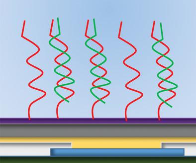
Arrays of field‐effect transistors are fabricated from chemical vapor deposition grown graphene (GFETs) and label‐free detection of DNA hybridization performed down to femtomolar concentrations. A process is developed for large‐area graphene sheets, which includes a thin Al2O3 layer, protecting the graphene from contamination during photolithographic patterning and a SiOx capping for biocompatibility. It enables fabrication of high‐quality transistor arrays, exhibiting stable close‐to‐zero Dirac point voltages under ambient conditions. Passivation of the as‐fabricated chip with a layer composed of two different oxides avoids direct electrochemical contact between the DNA solutions and the graphene layer during hybridization detection. DNA probe molecules are electrostatically immobilized via poly‐l‐lysine coating of the chip surface. Adsorption of this positively charged polymer induces a positive shift of the Dirac point and subsequent immobilization of negatively charged DNA probes induces a negative shift. Spatially resolved hybridization of DNA sequences is performed on the GFET arrays. End‐point as well as real‐time in situ measurements of hybridization are achieved. A detection limit of 10 fm is observed for hybridization of 20‐nucleotide DNA targets. Typical voltage signals are around 100 mV and spurious drifts below 1 mV per hour.
中文翻译:

用石墨烯晶体管阵列测量的DNA杂交。
场效应晶体管阵列由化学气相沉积生长的石墨烯(GFET)制成,并在低至飞摩尔浓度的情况下对DNA杂交进行无标记检测。开发了一种用于大面积石墨烯片的工艺,该工艺包括一个薄的Al 2 O 3层,可防止石墨烯在光刻图形化过程中受到污染并形成SiO x限制生物相容性。它可以制造高质量的晶体管阵列,并在环境条件下表现出稳定的接近零狄拉克点电压。用两种不同氧化物组成的层钝化制成的芯片可避免杂交检测过程中DNA溶液与石墨烯层之间的直接电化学接触。DNA探针分子通过静电聚固定升芯片表面的赖氨酸涂层。这种带正电的聚合物的吸附引起狄拉克点的正向移动,随后带负电的DNA探针的固定引起负向移动。在GFET阵列上进行DNA序列的空间分辨杂交。可以实现杂交的终点和实时原位测量。20个核苷酸DNA靶标的杂交检测限为10 f m。典型的电压信号约为100 mV,杂散漂移低于每小时1 mV。
更新日期:2020-08-19
中文翻译:
用石墨烯晶体管阵列测量的DNA杂交。
场效应晶体管阵列由化学气相沉积生长的石墨烯(GFET)制成,并在低至飞摩尔浓度的情况下对DNA杂交进行无标记检测。开发了一种用于大面积石墨烯片的工艺,该工艺包括一个薄的Al 2 O 3层,可防止石墨烯在光刻图形化过程中受到污染并形成SiO x限制生物相容性。它可以制造高质量的晶体管阵列,并在环境条件下表现出稳定的接近零狄拉克点电压。用两种不同氧化物组成的层钝化制成的芯片可避免杂交检测过程中DNA溶液与石墨烯层之间的直接电化学接触。DNA探针分子通过静电聚固定升芯片表面的赖氨酸涂层。这种带正电的聚合物的吸附引起狄拉克点的正向移动,随后带负电的DNA探针的固定引起负向移动。在GFET阵列上进行DNA序列的空间分辨杂交。可以实现杂交的终点和实时原位测量。20个核苷酸DNA靶标的杂交检测限为10 f m。典型的电压信号约为100 mV,杂散漂移低于每小时1 mV。


 京公网安备 11010802027423号