当前位置:
X-MOL 学术
›
Prog. Photovoltaics
›
论文详情
Our official English website, www.x-mol.net, welcomes your
feedback! (Note: you will need to create a separate account there.)
Green scalable vapor texture etching for multicrystalline silicon wafers
Progress in Photovoltaics ( IF 8.0 ) Pub Date : 2020-06-28 , DOI: 10.1002/pip.3302 Pei‐Yu Sun, Pi‐Chen Tsai, Po‐Yu Liang, Hsiao‐Ping Hsu, Agustina Sutejo, Allen Yang, Chung‐Wen Lan
Progress in Photovoltaics ( IF 8.0 ) Pub Date : 2020-06-28 , DOI: 10.1002/pip.3302 Pei‐Yu Sun, Pi‐Chen Tsai, Po‐Yu Liang, Hsiao‐Ping Hsu, Agustina Sutejo, Allen Yang, Chung‐Wen Lan
|
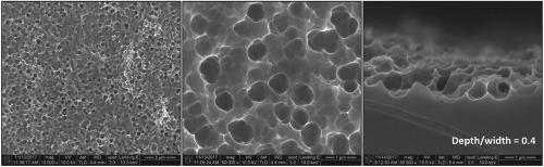
In recent years, the low‐cost diamond‐wire (DW) slicing has been widely used for single‐crystalline silicon (sc‐Si) wafers, and this makes sc‐Si solar cells very attractive to the market. On the contrary, the adoption of DW slicing for multicrystalline (mc‐Si) wafers is troublesome because of poor texturing quality in the existing production lines using acid solutions. We have developed a vapor texture etching (VTE) process with the combination of both acid and reacted vapors for DW sliced mc‐Si wafers. The etching process was rather simple and low cost. More importantly, the acid usage was low and recyclable, so that the acid emission was low as well. Its scale‐up was easy and straightforward. In this lab‐scale reactor, more than 50 full‐size wafers could be processed each time. The etched wafers had uniform appearance and low reflectivity, around 10%. After the nanostructure pores were enlarged by post treatments to minimize surface recombination, the full‐size mc‐Si solar cell fabricated by Solartech could achieve an efficiency of 19.7% using the Passivated Emitter and Rear Contact (PERC) structure, which was comparable with the average production efficiency.
中文翻译:

用于多晶硅晶片的绿色可扩展气相纹理蚀刻
近年来,低成本金刚石线(DW)切片已广泛用于单晶硅(sc-Si)晶圆,这使sc-Si太阳能电池对市场非常有吸引力。相反,由于在现有使用酸溶液的生产线中纹理质量差,因此在多晶(mc-Si)晶片上采用DW切片很麻烦。我们已经开发出一种结合了酸和反应后的蒸气的气相织构蚀刻(VTE)工艺,用于DW切片的mc-Si晶片。蚀刻工艺相当简单且成本低。更重要的是,酸用量低且可回收,因此酸排放量也低。它的放大非常简单明了。在这个实验室规模的反应器中,每次可以处理50多个全尺寸晶圆。蚀刻后的晶圆具有均匀的外观和低反射率,大约10%。通过后处理扩大纳米结构的孔隙以最大程度地减少表面重组后,采用钝化的发射极和后接触(PERC)结构,由Solartech制造的全尺寸mc-Si太阳能电池可以达到19.7%的效率,这可与之媲美。平均生产效率。
更新日期:2020-06-28
中文翻译:
用于多晶硅晶片的绿色可扩展气相纹理蚀刻
近年来,低成本金刚石线(DW)切片已广泛用于单晶硅(sc-Si)晶圆,这使sc-Si太阳能电池对市场非常有吸引力。相反,由于在现有使用酸溶液的生产线中纹理质量差,因此在多晶(mc-Si)晶片上采用DW切片很麻烦。我们已经开发出一种结合了酸和反应后的蒸气的气相织构蚀刻(VTE)工艺,用于DW切片的mc-Si晶片。蚀刻工艺相当简单且成本低。更重要的是,酸用量低且可回收,因此酸排放量也低。它的放大非常简单明了。在这个实验室规模的反应器中,每次可以处理50多个全尺寸晶圆。蚀刻后的晶圆具有均匀的外观和低反射率,大约10%。通过后处理扩大纳米结构的孔隙以最大程度地减少表面重组后,采用钝化的发射极和后接触(PERC)结构,由Solartech制造的全尺寸mc-Si太阳能电池可以达到19.7%的效率,这可与之媲美。平均生产效率。


 京公网安备 11010802027423号