当前位置:
X-MOL 学术
›
Mater. Horiz.
›
论文详情
Our official English website, www.x-mol.net, welcomes your
feedback! (Note: you will need to create a separate account there.)
Real-time monitoring of trap dynamics reveals the electronic states that limit charge transport in crystalline organic semiconductors
Materials Horizons ( IF 12.2 ) Pub Date : 2020-06-24 , DOI: 10.1039/d0mh00706d Hamna F. Iqbal 1, 2, 3, 4 , Emma K. Holland 4, 5, 6, 7 , John E. Anthony 4, 5, 6, 7 , Oana D. Jurchescu 1, 2, 3, 4
Materials Horizons ( IF 12.2 ) Pub Date : 2020-06-24 , DOI: 10.1039/d0mh00706d Hamna F. Iqbal 1, 2, 3, 4 , Emma K. Holland 4, 5, 6, 7 , John E. Anthony 4, 5, 6, 7 , Oana D. Jurchescu 1, 2, 3, 4
Affiliation
|
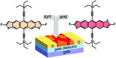
Organic semiconductors (OSCs) have the potential to become ubiquitous in our lives as part of various optoelectronic devices given their low-cost processing, light weight, and the opportunities that they offer for designing new materials with “on demand” properties. Many OSCs have achieved remarkable performances, however, a complete understanding of the fundamental processes that govern their properties is still lacking. One such process is charge carrier trapping, a phenomenon that profoundly impacts the performance and stability of devices. Here we report on a comprehensive study on the physics of traps resulting from microstructure changes by monitoring the generation/annihilation of traps in 2,8-difluoro-5,11-bis(triethylsilylethynyl)anthradithiophene (diF-TES ADT), a high-mobility small molecule OSC. The variations in charge carrier mobility measured in organic field-effect transistors (OFETs) deliberately exposed to solvent vapor are correlated with the density and energetic distribution of the electronic states in the band gap of the OSC in all intermediate states of the microstructural transformations. Given the strong dependence of the electrical properties on the film microstructure, such information is instrumental in identifying performance-limiting processes in devices and subsequently guiding material processing to achieve intrinsic limits. The discovery of defect-tolerant intermediate crystalline motifs may provide new pathways for fabricating stable, high-performance devices for next-generation low-cost electronics.
中文翻译:

陷阱动态监测的实时监测揭示了限制晶体有机半导体中电荷传输的电子状态
有机半导体(OSC)具有低成本制造,重量轻以及为设计具有“按需”特性的新材料提供的机会,因此有可能成为我们生活中无处不在的各种光电设备的一部分。许多OSC取得了卓越的性能,但是,仍然缺乏对控制其特性的基本过程的全面了解。一种这样的过程是电荷载流子捕获,这种现象深刻影响器件的性能和稳定性。在这里,我们通过监测2,8-二氟-5,11-双(三乙基甲硅烷基乙炔基)蒽噻吩(diF-TES ADT)中的陷阱的产生/ an灭,对由微观结构变化导致的陷阱的物理现象进行了全面研究。流动性小分子OSC。在有机场效应晶体管(OFET)故意暴露于溶剂蒸汽中测得的电荷载流子迁移率变化与微结构转变的所有中间状态下OSC带隙中电子态的密度和高能分布相关。考虑到电性能对薄膜微结构的强烈依赖性,此类信息有助于识别设备中的性能限制过程,并随后指导材料加工以达到固有极限。耐缺陷的中间晶体图案的发现可能为制造用于下一代低成本电子产品的稳定,高性能的设备提供新的途径。
更新日期:2020-09-01
中文翻译:
陷阱动态监测的实时监测揭示了限制晶体有机半导体中电荷传输的电子状态
有机半导体(OSC)具有低成本制造,重量轻以及为设计具有“按需”特性的新材料提供的机会,因此有可能成为我们生活中无处不在的各种光电设备的一部分。许多OSC取得了卓越的性能,但是,仍然缺乏对控制其特性的基本过程的全面了解。一种这样的过程是电荷载流子捕获,这种现象深刻影响器件的性能和稳定性。在这里,我们通过监测2,8-二氟-5,11-双(三乙基甲硅烷基乙炔基)蒽噻吩(diF-TES ADT)中的陷阱的产生/ an灭,对由微观结构变化导致的陷阱的物理现象进行了全面研究。流动性小分子OSC。在有机场效应晶体管(OFET)故意暴露于溶剂蒸汽中测得的电荷载流子迁移率变化与微结构转变的所有中间状态下OSC带隙中电子态的密度和高能分布相关。考虑到电性能对薄膜微结构的强烈依赖性,此类信息有助于识别设备中的性能限制过程,并随后指导材料加工以达到固有极限。耐缺陷的中间晶体图案的发现可能为制造用于下一代低成本电子产品的稳定,高性能的设备提供新的途径。


 京公网安备 11010802027423号