当前位置:
X-MOL 学术
›
ACS Appl. Mater. Interfaces
›
论文详情
Our official English website, www.x-mol.net, welcomes your
feedback! (Note: you will need to create a separate account there.)
Catalyst-Free Growth of Two-Dimensional BCxN Materials on Dielectrics by Temperature-Dependent Plasma-Enhanced Chemical Vapor Deposition.
ACS Applied Materials & Interfaces ( IF 8.3 ) Pub Date : 2020-06-23 , DOI: 10.1021/acsami.0c08555 Kongyang Yi 1, 2, 3 , Zhepeng Jin 1, 2 , Saiyu Bu 4 , Dingguan Wang 5 , Donghua Liu 1, 2 , Yamin Huang 3 , Yemin Dong 3 , Qinghong Yuan 4 , Yunqi Liu 2 , Andrew Thye Shen Wee 5 , Dacheng Wei 1, 2
ACS Applied Materials & Interfaces ( IF 8.3 ) Pub Date : 2020-06-23 , DOI: 10.1021/acsami.0c08555 Kongyang Yi 1, 2, 3 , Zhepeng Jin 1, 2 , Saiyu Bu 4 , Dingguan Wang 5 , Donghua Liu 1, 2 , Yamin Huang 3 , Yemin Dong 3 , Qinghong Yuan 4 , Yunqi Liu 2 , Andrew Thye Shen Wee 5 , Dacheng Wei 1, 2
Affiliation
|
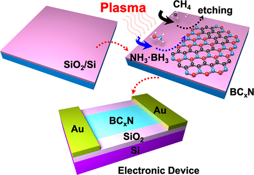
Traditional methods to prepare two-dimensional (2D) B–C–N ternary materials (BCxN), such as chemical vapor deposition (CVD), require sophisticated experimental conditions such as high temperature, delicate control of precursors, and postgrowth transfer from catalytic substrates, and the products are generally thick or bulky films without the atomically mixed phase of B–C–N, hampering practical applications of these materials. Here, for the first time, we develop a temperature-dependent plasma-enhanced chemical vapor deposition (PECVD) method to grow 2D BCxN materials directly on noncatalytic dielectrics at low temperature with high controllability. The C, N, and B compositions can be tuned by simply changing the growth temperature. Thus, the properties of the as-made materials including band gap and conductivity are modulated, which is hardly achieved by other methods. A 2D hybridized BC2N film with a mixed BC2N phase is produced, for the first time, with a band gap of about 2.3 eV. The growth temperature is 580–620 °C, much lower than that of traditional catalytic CVD for growing BCxN. The product has a p-type conducting property and can be directly applied in field-effect transistors and sensors without postgrowth transfer, showing great promise for this method in future applications.
中文翻译:

温度依赖性等离子体增强化学气相沉积法在电介质上二维BCxN材料无催化剂生长。
制备二维(2D)B–C–N三元材料(BC x N)的传统方法,例如化学气相沉积(CVD),需要复杂的实验条件,例如高温,对前驱物的精细控制以及从催化底物,产品通常是厚的或大体积的薄膜,没有B–C–N的原子混合相,这妨碍了这些材料的实际应用。在这里,我们首次开发了一种依赖于温度的等离子体增强化学气相沉积(PECVD)方法来生长2D BC xN材料在低温下直接以非催化电介质具有高可控性。可以通过简单地改变生长温度来调节C,N和B的组成。因此,所制成材料的性能,包括带隙和电导率,得到了调节,这是其他方法很难实现的。首次生产出具有BC 2 N混合相的2D杂交BC 2 N薄膜,其带隙约为2.3 eV。生长温度为580–620°C,远低于用于生长BC x N的传统催化CVD温度。该产品具有p型导电性能,可直接应用于场效应晶体管和传感器,而无需生长后转移,这表明这种方法在未来的应用中很有希望。
更新日期:2020-07-22
中文翻译:
温度依赖性等离子体增强化学气相沉积法在电介质上二维BCxN材料无催化剂生长。
制备二维(2D)B–C–N三元材料(BC x N)的传统方法,例如化学气相沉积(CVD),需要复杂的实验条件,例如高温,对前驱物的精细控制以及从催化底物,产品通常是厚的或大体积的薄膜,没有B–C–N的原子混合相,这妨碍了这些材料的实际应用。在这里,我们首次开发了一种依赖于温度的等离子体增强化学气相沉积(PECVD)方法来生长2D BC xN材料在低温下直接以非催化电介质具有高可控性。可以通过简单地改变生长温度来调节C,N和B的组成。因此,所制成材料的性能,包括带隙和电导率,得到了调节,这是其他方法很难实现的。首次生产出具有BC 2 N混合相的2D杂交BC 2 N薄膜,其带隙约为2.3 eV。生长温度为580–620°C,远低于用于生长BC x N的传统催化CVD温度。该产品具有p型导电性能,可直接应用于场效应晶体管和传感器,而无需生长后转移,这表明这种方法在未来的应用中很有希望。


 京公网安备 11010802027423号