当前位置:
X-MOL 学术
›
Adv. Electron. Mater.
›
论文详情
Our official English website, www.x-mol.net, welcomes your
feedback! (Note: you will need to create a separate account there.)
Atomically Controlled Tunable Doping in High‐Performance WSe2 Devices
Advanced Electronic Materials ( IF 5.3 ) Pub Date : 2020-06-21 , DOI: 10.1002/aelm.201901304 Chin‐Sheng Pang 1 , Terry Y. T. Hung 1 , Ava Khosravi 2 , Rafik Addou 2, 3 , Qingxiao Wang 2 , Moon J. Kim 2 , Robert M. Wallace 2 , Zhihong Chen 1
Advanced Electronic Materials ( IF 5.3 ) Pub Date : 2020-06-21 , DOI: 10.1002/aelm.201901304 Chin‐Sheng Pang 1 , Terry Y. T. Hung 1 , Ava Khosravi 2 , Rafik Addou 2, 3 , Qingxiao Wang 2 , Moon J. Kim 2 , Robert M. Wallace 2 , Zhihong Chen 1
Affiliation
|
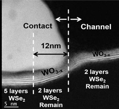
2D transitional metal dichalcogenide (TMD) field‐effect transistors are promising candidates for future electronic applications, owing to their potential for ultimate device scaling. However, it is acknowledged that substantial contact resistance associated with the contact‐TMD interface has impeded device performance to a large extent. It has been discovered that O2 plasma treatment can convert WSe2 into WO3−x and substantially improve contact resistances of p‐type WSe2 devices by strong doping induced thinner depletion width. In this paper, temperature dependence of this conversion is studied, demonstrating an oxidation process with a precise monolayer control at room temperature and multilayer conversion at elevated temperatures. Furthermore, lateral oxidation of WSe2 underneath contact revealed by high‐resolution scanning transmission electron microscope leads to potential unpinning of the metal Fermi level and Schottky barrier lowering, resulting in lower contact resistances. The p‐doping effect is attributed to the high electron affinity of the WO3−x layer on top of the remaining WSe2 channel, and the doping level is dependent on the WO3−x thickness that is controlled by the temperature. Comprehensive materials and electrical characterizations are presented, with a low contact resistance of ≈528 Ω μm and record high on‐state current of 320 μA μm−1 at −1 V bias being reported.
中文翻译:

高性能WSe2器件中的原子控制可调掺杂
由于2D过渡金属二硫化碳(TMD)场效应晶体管具有最终器件规模化的潜力,因此它们有望成为未来电子应用的候选材料。但是,公认的是,与contact-TMD接口相关的大量接触电阻已在很大程度上阻碍了设备性能。已经发现,O 2等离子体处理可以将WSe 2转化为WO 3- x 并显着提高p型WSe 2的接触电阻器件通过强掺杂引起更薄的耗尽层宽度。在本文中,研究了这种转化的温度依赖性,证明了在室温下具有精确的单层控制并在高温下具有多层转化的氧化过程。此外,高分辨率扫描透射电子显微镜揭示的接触下方WSe 2的侧向氧化会导致金属费米能级的未固定和肖特基势垒降低,从而导致较低的接触电阻。p掺杂效应归因于剩余WSe 2通道顶部的WO 3- x 层的高电子亲和力,并且掺杂水平取决于WO 3- x 由温度控制的厚度。全面的材料和电表征被呈现,具有≈528Ω微米,320个微米μA记录高导通电流低的接触电阻-1被报告在-1V的偏压。
更新日期:2020-08-10
中文翻译:
高性能WSe2器件中的原子控制可调掺杂
由于2D过渡金属二硫化碳(TMD)场效应晶体管具有最终器件规模化的潜力,因此它们有望成为未来电子应用的候选材料。但是,公认的是,与contact-TMD接口相关的大量接触电阻已在很大程度上阻碍了设备性能。已经发现,O 2等离子体处理可以将WSe 2转化为WO 3- x 并显着提高p型WSe 2的接触电阻器件通过强掺杂引起更薄的耗尽层宽度。在本文中,研究了这种转化的温度依赖性,证明了在室温下具有精确的单层控制并在高温下具有多层转化的氧化过程。此外,高分辨率扫描透射电子显微镜揭示的接触下方WSe 2的侧向氧化会导致金属费米能级的未固定和肖特基势垒降低,从而导致较低的接触电阻。p掺杂效应归因于剩余WSe 2通道顶部的WO 3- x 层的高电子亲和力,并且掺杂水平取决于WO 3- x 由温度控制的厚度。全面的材料和电表征被呈现,具有≈528Ω微米,320个微米μA记录高导通电流低的接触电阻-1被报告在-1V的偏压。


 京公网安备 11010802027423号