当前位置:
X-MOL 学术
›
ACS Photonics
›
论文详情
Our official English website, www.x-mol.net, welcomes your
feedback! (Note: you will need to create a separate account there.)
Fractal Shaped Periodic Metal Nanostructures Atop Dielectric-Metal Substrates for SERS Applications
ACS Photonics ( IF 6.5 ) Pub Date : 2020-06-16 , DOI: 10.1021/acsphotonics.0c00257 Sergey M. Novikov 1, 2 , Sergejs Boroviks 2 , Andrey B. Evlyukhin 1, 3 , Dmitry E. Tatarkin 1 , Aleksey V. Arsenin 1 , Valentyn S. Volkov 1 , Sergey I. Bozhevolnyi 2, 4
ACS Photonics ( IF 6.5 ) Pub Date : 2020-06-16 , DOI: 10.1021/acsphotonics.0c00257 Sergey M. Novikov 1, 2 , Sergejs Boroviks 2 , Andrey B. Evlyukhin 1, 3 , Dmitry E. Tatarkin 1 , Aleksey V. Arsenin 1 , Valentyn S. Volkov 1 , Sergey I. Bozhevolnyi 2, 4
Affiliation
|
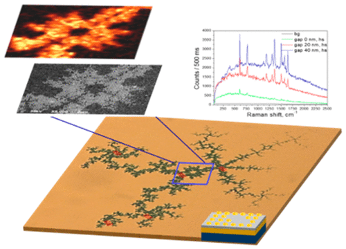
Controlled and reliable field enhancement (FE) effects associated with the excitation of plasmons in resonant metal nanostructures constitute an essential prerequisite for the development of various sensing configurations, especially those utilizing surface-enhanced Raman scattering (SERS) spectroscopy techniques. Leveraging advantages of random nanostructures in providing strong collective resonances in a broad wavelength range with the design flexibility of individual gap plasmon resonators, we experimentally investigate fractal-shaped arrays of gap plasmon resonators and characterize the occurring FE effects by mapping SERS signals from uniformly spread Rhodamine 6G with high-resolution Raman microscopy. In such a geometry, the total FE is expected to benefit from both FE associated with gap plasmon excitation and FE due to constructive interference of the surface plasmon modes reflected and diffracted by fractal-shaped boundaries. Linear reflection imaging spectroscopy is used to verify that the fabricated nanostructures exhibit spatially distributed resonances (bright spots) close to the excitation wavelengths used for the Raman microscopy. The positions of bright spots are argued to be influenced by fractal-shaped boundaries, particle dimensions, polarization, and wavelength of the incident and scattered light. Experimentally obtained SERS images from similar fractal (gold) structures fabricated with different dielectric SiO2 spacer thicknesses (0, 20, and 40 nm) featured diffraction-limited bright spots corresponding to local SERS enhancements of up to ∼107 (relative to Raman signals obtained with a glass substrate) for 40 nm thick SiO2 layers. Our results indicate that the strategy of combining fractal array geometry with gap plasmon resonances is promising for the design of highly efficient SERS substrates for potential applications in surface-enhanced multichannel sensing, including single-molecule spectroscopy.
中文翻译:

用于SERS应用的介电金属衬底上的分形周期性金属纳米结构
与共振金属纳米结构中的等离激元激发相关的受控且可靠的场增强(FE)效应,构成了开发各种传感配置(尤其是利用表面增强拉曼散射(SERS)光谱技术的传感配置)的必要先决条件。利用随机纳米结构的优势,可以在宽的波长范围内提供强的集体共振以及各个间隙等离子体激元谐振器的设计灵活性,我们通过实验研究间隙等离子体激元谐振器的分形阵列,并通过映射来自均匀扩散的罗丹明的SERS信号来表征发生的有限元效应具有高分辨率拉曼显微镜的6G。在这样的几何形状中 由于分形形边界反射和衍射的表面等离激元模式的相长干涉,总的有限元有望从与间隙等离激元激发相关的FE和FE中受益。线性反射成像光谱法用于验证所制造的纳米结构在空间分布上的共振(亮点)接近拉曼显微镜所用的激发波长。据认为,亮点的位置受分形边界,粒子尺寸,偏振以及入射光和散射光的波长的影响。从不同电介质SiO制备的类似分形(金)结构中获得的实验SERS图像 线性反射成像光谱法用于验证所制造的纳米结构在空间分布上的共振(亮点)接近拉曼显微镜所用的激发波长。据认为,亮点的位置受分形边界,粒子尺寸,偏振以及入射光和散射光的波长的影响。从不同电介质SiO制备的类似分形(金)结构中获得的实验SERS图像 线性反射成像光谱法用于验证所制造的纳米结构在空间分布上的共振(亮点)接近拉曼显微镜所用的激发波长。据认为,亮点的位置受分形边界,粒子尺寸,偏振以及入射光和散射光的波长的影响。从不同电介质SiO制备的类似分形(金)结构中获得的实验SERS图像2个间隔物厚度(0、20和40 nm)具有衍射限制的亮点,对应于40 nm厚SiO 2层的局部SERS增强高达〜10 7(相对于玻璃基板获得的拉曼信号)。我们的结果表明,将分形阵列的几何形状与间隙等离子体激元共振相结合的策略对于设计高效SERS底物具有广阔的前景,包括潜在的应用在表面增强的多通道传感(包括单分子光谱)中。
更新日期:2020-07-15
中文翻译:
用于SERS应用的介电金属衬底上的分形周期性金属纳米结构
与共振金属纳米结构中的等离激元激发相关的受控且可靠的场增强(FE)效应,构成了开发各种传感配置(尤其是利用表面增强拉曼散射(SERS)光谱技术的传感配置)的必要先决条件。利用随机纳米结构的优势,可以在宽的波长范围内提供强的集体共振以及各个间隙等离子体激元谐振器的设计灵活性,我们通过实验研究间隙等离子体激元谐振器的分形阵列,并通过映射来自均匀扩散的罗丹明的SERS信号来表征发生的有限元效应具有高分辨率拉曼显微镜的6G。在这样的几何形状中 由于分形形边界反射和衍射的表面等离激元模式的相长干涉,总的有限元有望从与间隙等离激元激发相关的FE和FE中受益。线性反射成像光谱法用于验证所制造的纳米结构在空间分布上的共振(亮点)接近拉曼显微镜所用的激发波长。据认为,亮点的位置受分形边界,粒子尺寸,偏振以及入射光和散射光的波长的影响。从不同电介质SiO制备的类似分形(金)结构中获得的实验SERS图像 线性反射成像光谱法用于验证所制造的纳米结构在空间分布上的共振(亮点)接近拉曼显微镜所用的激发波长。据认为,亮点的位置受分形边界,粒子尺寸,偏振以及入射光和散射光的波长的影响。从不同电介质SiO制备的类似分形(金)结构中获得的实验SERS图像 线性反射成像光谱法用于验证所制造的纳米结构在空间分布上的共振(亮点)接近拉曼显微镜所用的激发波长。据认为,亮点的位置受分形边界,粒子尺寸,偏振以及入射光和散射光的波长的影响。从不同电介质SiO制备的类似分形(金)结构中获得的实验SERS图像2个间隔物厚度(0、20和40 nm)具有衍射限制的亮点,对应于40 nm厚SiO 2层的局部SERS增强高达〜10 7(相对于玻璃基板获得的拉曼信号)。我们的结果表明,将分形阵列的几何形状与间隙等离子体激元共振相结合的策略对于设计高效SERS底物具有广阔的前景,包括潜在的应用在表面增强的多通道传感(包括单分子光谱)中。


 京公网安备 11010802027423号