当前位置:
X-MOL 学术
›
Adv. Opt. Mater.
›
论文详情
Our official English website, www.x-mol.net, welcomes your
feedback! (Note: you will need to create a separate account there.)
Selective and Sensitive Photon Sieve Based on III–V Semiconductor Nanowire Forest Fabricated by Lithography‐Free Process
Advanced Optical Materials ( IF 8.0 ) Pub Date : 2020-06-15 , DOI: 10.1002/adom.202000198 Gil Ju Lee 1 , Kwangwook Park 2 , Min Seok Kim 1 , Sehui Chang 1 , Tae Joon Seok 1 , Hong‐Gyu Park 3 , Gunwu Ju 4 , Kyujung Kim 5 , Young Min Song 1
Advanced Optical Materials ( IF 8.0 ) Pub Date : 2020-06-15 , DOI: 10.1002/adom.202000198 Gil Ju Lee 1 , Kwangwook Park 2 , Min Seok Kim 1 , Sehui Chang 1 , Tae Joon Seok 1 , Hong‐Gyu Park 3 , Gunwu Ju 4 , Kyujung Kim 5 , Young Min Song 1
Affiliation
|
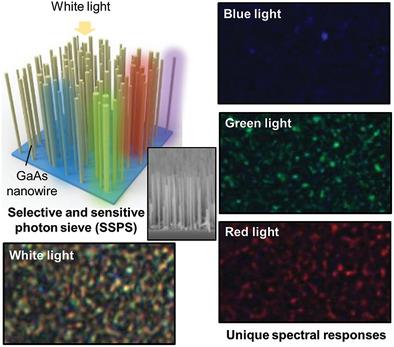
Vertically oriented semiconductor nanowires (NWs) have been intensely studied in macroscopic perspective due to their attractive applications such as optical filters, photodiodes, and solar cells. However, microscopic photonic phenomena of dense and random NWs have been rarely, and their promising applications have not been explored. Therefore, this article theoretically and experimentally investigates the microscopic photonic event of dense and random NWs using highly selective and sensitive photon sieve (SSPS), which employs highly populated III/V semiconductor NW forests fabricated with a lithography‐free self‐catalyzed growth method. Theoretical analyses reveal that diameter‐dependent and selective photon absorption occurs even for a dense and disordered NW distribution. The engineered growth process affords highly populated NW forests (mean shortest interval = 192.4 nm) comprising NWs with a high aspect ratio (mean aspect ratio = 34.3) and a sufficiently broad diameter distribution to span the visible spectrum and decompose it (mean diameter = 94 nm, standard deviation = 49 nm). Moreover, the SSPS exhibits unique spectral responses to monochromatic light of different wavelengths (correlation coefficients < 0.03) and a high sensitivity with a highest absorptivity of 92.4%. This work indicates SSPSs can be utilized for various applications of artificial photoreceptor, physically unclonable function, and high efficient optoelectronics.
中文翻译:

无光刻工艺制备的基于III-V族半导体纳米线森林的选择性灵敏光子筛
垂直取向的半导体纳米线(NWs)由于其吸引人的应用(例如滤光片,光电二极管和太阳能电池)已在宏观角度进行了深入研究。但是,密集和随机西北面的微观光子现象很少见,尚未探索其有前途的应用。因此,本文在理论上和实验上使用高选择性和灵敏的光子筛(SSPS)研究了密集和随机NW的微观光子事件,该方法采用了采用无光刻自催化生长方法制备的高密度III / V半导体NW森林。理论分析表明,即使对于密集且无序的NW分布,也会发生直径相关的选择性光子吸收。经过精心设计的生长过程可提供人口稠密的西北森林(平均最短间隔= 192.4 nm),其中包括具有高纵横比(平均纵横比= 34.3)和足够宽的直径分布以覆盖可见光谱并分解(平均直径= 94)的NW nm,标准偏差= 49 nm)。此外,SSPS对不同波长的单色光(相关系数<0.03)表现出独特的光谱响应,并具有高达92.4%的最高吸收率的高灵敏度。这项工作表明SSPS可以用于人造感光体,物理不可克隆的功能和高效光电的各种应用。3)和足够宽的直径分布以覆盖可见光谱并分解(平均直径= 94 nm,标准偏差= 49 nm)。此外,SSPS对不同波长的单色光(相关系数<0.03)表现出独特的光谱响应,并具有高达92.4%的最高吸收率的高灵敏度。这项工作表明SSPS可以用于人造感光体,物理不可克隆的功能和高效光电的各种应用。3)和足够宽的直径分布以覆盖可见光谱并分解(平均直径= 94 nm,标准偏差= 49 nm)。此外,SSPS对不同波长的单色光(相关系数<0.03)表现出独特的光谱响应,并具有高达92.4%的最高吸收率的高灵敏度。这项工作表明SSPS可以用于人造感光体,物理不可克隆的功能和高效光电的各种应用。
更新日期:2020-06-15
中文翻译:
无光刻工艺制备的基于III-V族半导体纳米线森林的选择性灵敏光子筛
垂直取向的半导体纳米线(NWs)由于其吸引人的应用(例如滤光片,光电二极管和太阳能电池)已在宏观角度进行了深入研究。但是,密集和随机西北面的微观光子现象很少见,尚未探索其有前途的应用。因此,本文在理论上和实验上使用高选择性和灵敏的光子筛(SSPS)研究了密集和随机NW的微观光子事件,该方法采用了采用无光刻自催化生长方法制备的高密度III / V半导体NW森林。理论分析表明,即使对于密集且无序的NW分布,也会发生直径相关的选择性光子吸收。经过精心设计的生长过程可提供人口稠密的西北森林(平均最短间隔= 192.4 nm),其中包括具有高纵横比(平均纵横比= 34.3)和足够宽的直径分布以覆盖可见光谱并分解(平均直径= 94)的NW nm,标准偏差= 49 nm)。此外,SSPS对不同波长的单色光(相关系数<0.03)表现出独特的光谱响应,并具有高达92.4%的最高吸收率的高灵敏度。这项工作表明SSPS可以用于人造感光体,物理不可克隆的功能和高效光电的各种应用。3)和足够宽的直径分布以覆盖可见光谱并分解(平均直径= 94 nm,标准偏差= 49 nm)。此外,SSPS对不同波长的单色光(相关系数<0.03)表现出独特的光谱响应,并具有高达92.4%的最高吸收率的高灵敏度。这项工作表明SSPS可以用于人造感光体,物理不可克隆的功能和高效光电的各种应用。3)和足够宽的直径分布以覆盖可见光谱并分解(平均直径= 94 nm,标准偏差= 49 nm)。此外,SSPS对不同波长的单色光(相关系数<0.03)表现出独特的光谱响应,并具有高达92.4%的最高吸收率的高灵敏度。这项工作表明SSPS可以用于人造感光体,物理不可克隆的功能和高效光电的各种应用。


 京公网安备 11010802027423号