当前位置:
X-MOL 学术
›
ACS Appl. Nano Mater.
›
论文详情
Our official English website, www.x-mol.net, welcomes your
feedback! (Note: you will need to create a separate account there.)
Visible Phototransistors Based on Vertical Nanolayered Heterostructures of SnS/SnS2 p–n and SnSe2/SnS2 n–n Nanoflakes
ACS Applied Nano Materials ( IF 5.3 ) Pub Date : 2020-06-12 , DOI: 10.1021/acsanm.0c01213 He Tian 1 , Xiancheng Meng 1 , Juehan Yang 2 , Chao Fan 1, 3 , Shuo Yuan 1 , Xia An 1 , Chun Sun 1 , Yonghui Zhang 1 , Mengjun Wang 1 , Hongxing Zheng 1 , Zhongming Wei 2 , Erping Li 3
ACS Applied Nano Materials ( IF 5.3 ) Pub Date : 2020-06-12 , DOI: 10.1021/acsanm.0c01213 He Tian 1 , Xiancheng Meng 1 , Juehan Yang 2 , Chao Fan 1, 3 , Shuo Yuan 1 , Xia An 1 , Chun Sun 1 , Yonghui Zhang 1 , Mengjun Wang 1 , Hongxing Zheng 1 , Zhongming Wei 2 , Erping Li 3
Affiliation
|
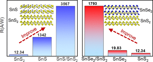
Two-dimensional (2D) nanomaterials have been attracting intensive interest due to their unique physical and optoelectronic properties. Van der Waals nanolayered heterostructures based on different 2D nanomaterials provide a state-of-the-art platform for investigating the physical phenomena and have extended the applications of 2D nanomaterials, leading to an era of next-generation high-performance electronic and optoelectronic technology. Herein, vertical 2D SnS/SnS2 p–n and SnSe2/SnS2 n–n nanolayered heterostructures are constructed by exfoliating individual materials and stacking them artificially. The two types of back-gate field-effect phototransistors show clear rectifying behaviors with the existence of band offset and excellent optoelectronic performances. The SnS/SnS2 p–n nanolayered heterostructure shows an ambipolar behavior with a hole mobility of 6.96 cm2·V–1·s–1 and electron mobility of 0.68 cm2·V–1·s–1, while the SnSe2/SnS2 n–n nanolayered heterostructure shows an intense n-type behavior with electron mobility of 3.78 cm2·V–1·s–1 and a high on/off ratio of over 105. Interestingly, due to the band alignments and built-in potentials in the two types of nanolayered heterostructures, the phototransistors exhibit enhanced responsive performances to illuminations of three-primary-color lasers (λ = 405, 532, and 650 nm) compared to the individual components. The SnS/SnS2 phototransistor shows a high photoresponsivity of 3567 A W–1, a high detectivity of 3.64 × 10¹³ Jones, and a fast response time of 0.8 ms. The SnSe2/SnS2 phototransistor also exhibits a high photoresponsivity of 1793 A W–1 and a fast response time of 15.4 ms.
中文翻译:

基于SnS / SnS 2 p–n和SnSe 2 / SnS 2 n–n纳米薄片的垂直纳米层异质结构的可见光电晶体管
二维(2D)纳米材料因其独特的物理和光电特性而引起了广泛的关注。基于不同2D纳米材料的Van der Waals纳米层异质结构为研究物理现象提供了最先进的平台,并扩展了2D纳米材料的应用,从而导致了下一代高性能电子和光电技术时代。这里,垂直二维SnS / SnS 2 p–n和SnSe 2 / SnS 2n–n纳米层异质结构是通过剥离单个材料并将其人工堆叠而成的。两种类型的背栅场效应光电晶体管显示出清晰的整流行为,并存在带隙偏移和出色的光电性能。SnS / SnS 2 p–n纳米层异质结构表现出双极性行为,空穴迁移率为6.96 cm 2 ·V –1 ·s –1,电子迁移率为0.68 cm 2 ·V –1 ·s –1,而SnSe 2 / SnS 2 n–n纳米层异质结构表现出强烈的n型行为,电子迁移率为3.78 cm 2 ·V –1·s –1,高开/关比超过10 5。有趣的是,由于两种类型的纳米层异质结构中的能带排列和内在电势,与单个晶体管相比,光电晶体管对三基色激光(λ= 405、532和650 nm)的照明表现出增强的响应性能。组件。SnS / SnS 2光电晶体管显示出3567 AW –1的高光敏度,3.64×10 13 Jones的高检测度以及0.8 ms的快速响应时间。SnSe 2 / SnS 2光电晶体管还具有1793 AW –1的高光响应性和15.4 ms的快速响应时间。
更新日期:2020-07-24
中文翻译:
基于SnS / SnS 2 p–n和SnSe 2 / SnS 2 n–n纳米薄片的垂直纳米层异质结构的可见光电晶体管
二维(2D)纳米材料因其独特的物理和光电特性而引起了广泛的关注。基于不同2D纳米材料的Van der Waals纳米层异质结构为研究物理现象提供了最先进的平台,并扩展了2D纳米材料的应用,从而导致了下一代高性能电子和光电技术时代。这里,垂直二维SnS / SnS 2 p–n和SnSe 2 / SnS 2n–n纳米层异质结构是通过剥离单个材料并将其人工堆叠而成的。两种类型的背栅场效应光电晶体管显示出清晰的整流行为,并存在带隙偏移和出色的光电性能。SnS / SnS 2 p–n纳米层异质结构表现出双极性行为,空穴迁移率为6.96 cm 2 ·V –1 ·s –1,电子迁移率为0.68 cm 2 ·V –1 ·s –1,而SnSe 2 / SnS 2 n–n纳米层异质结构表现出强烈的n型行为,电子迁移率为3.78 cm 2 ·V –1·s –1,高开/关比超过10 5。有趣的是,由于两种类型的纳米层异质结构中的能带排列和内在电势,与单个晶体管相比,光电晶体管对三基色激光(λ= 405、532和650 nm)的照明表现出增强的响应性能。组件。SnS / SnS 2光电晶体管显示出3567 AW –1的高光敏度,3.64×10 13 Jones的高检测度以及0.8 ms的快速响应时间。SnSe 2 / SnS 2光电晶体管还具有1793 AW –1的高光响应性和15.4 ms的快速响应时间。


 京公网安备 11010802027423号