当前位置:
X-MOL 学术
›
Adv. Electron. Mater.
›
论文详情
Our official English website, www.x-mol.net, welcomes your
feedback! (Note: you will need to create a separate account there.)
High‐Performance On‐Chip Electron Sources Based on Electroformed Silicon Oxide
Advanced Electronic Materials ( IF 5.3 ) Pub Date : 2020-06-11 , DOI: 10.1002/aelm.202000268 Wei Yang 1 , Zhiwei Li 1 , Yuwei Wang 2 , Jun Shen 3 , Dapeng Wei 3 , Xianlong Wei 1
Advanced Electronic Materials ( IF 5.3 ) Pub Date : 2020-06-11 , DOI: 10.1002/aelm.202000268 Wei Yang 1 , Zhiwei Li 1 , Yuwei Wang 2 , Jun Shen 3 , Dapeng Wei 3 , Xianlong Wei 1
Affiliation
|
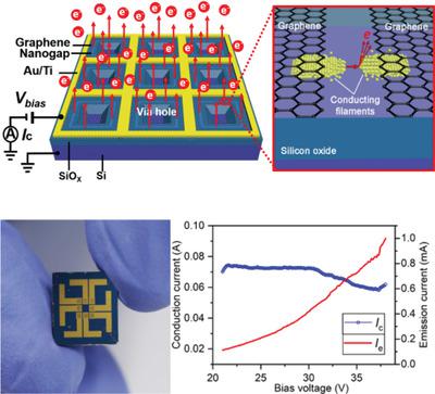
On‐chip electron sources with the advantages of high emission current and density, high emission efficiency, low working voltage, and easy fabrication are highly desired for scaling down free electron‐based devices and systems, especially for realizing those on a chip, but remain challenging. Here, such an on‐chip electron source is reported simply based on electroformed silicon oxide between concentric graphene films on silicon oxide substrate. It is demonstrated that electron emission from an electron emitter can be driven by a low voltage about 11 V, and a high emission efficiency of 33.6%. An on‐chip electron source with 36 × 36 emitter array in an area of 594 × 594 µm2 exhibits an emission current up to 1 mA at 38 V working voltage, corresponding to a high emission density of 283 mA cm−2. Electron emission from the sources is thought to be generated from horizontal tunneling diodes formed in electroformed silicon oxide. Combined advantages of high emission current and density, high emission efficiency, low working voltage, and easy fabrication make this on‐chip electron sources promising in realizing miniature and on‐chip free electron‐based devices and systems.
中文翻译:

基于电铸氧化硅的高性能片上电子源
为了缩小基于自由电子的器件和系统的规模,特别是为了实现芯片上的电子器件,具有高发射电流和高密度,高发射效率,低工作电压以及易于制造的片上电子源是迫切需要的。具有挑战性的。在此,仅基于氧化硅衬底上同心石墨烯膜之间的电铸氧化硅来报道这种片上电子源。已经证明,可以通过约11V的低电压和33.6%的高发射效率来驱动来自电子发射器的电子发射。具有594×594 µm 2面积的36×36发射器阵列的片上电子源在38 V工作电压下具有高达1 mA的发射电流,对应于283 mA cm -2的高发射密度。来自源的电子发射被认为是由在电铸氧化硅中形成的水平隧穿二极管产生的。高发射电流和高密度,高发射效率,低工作电压以及易于制造的综合优势,使得该片上电子源有望实现基于微型和片上自由电子的器件和系统。
更新日期:2020-07-13
中文翻译:
基于电铸氧化硅的高性能片上电子源
为了缩小基于自由电子的器件和系统的规模,特别是为了实现芯片上的电子器件,具有高发射电流和高密度,高发射效率,低工作电压以及易于制造的片上电子源是迫切需要的。具有挑战性的。在此,仅基于氧化硅衬底上同心石墨烯膜之间的电铸氧化硅来报道这种片上电子源。已经证明,可以通过约11V的低电压和33.6%的高发射效率来驱动来自电子发射器的电子发射。具有594×594 µm 2面积的36×36发射器阵列的片上电子源在38 V工作电压下具有高达1 mA的发射电流,对应于283 mA cm -2的高发射密度。来自源的电子发射被认为是由在电铸氧化硅中形成的水平隧穿二极管产生的。高发射电流和高密度,高发射效率,低工作电压以及易于制造的综合优势,使得该片上电子源有望实现基于微型和片上自由电子的器件和系统。


 京公网安备 11010802027423号