当前位置:
X-MOL 学术
›
Mater. Today Phys.
›
论文详情
Our official English website, www.x-mol.net, welcomes your
feedback! (Note: you will need to create a separate account there.)
Thickness dependent Carrier Lifetime and Mobility for MAPbBr3 Single Crystals
Materials Today Physics ( IF 10.0 ) Pub Date : 2020-08-01 , DOI: 10.1016/j.mtphys.2020.100240 J. Xing , Y. Zou , C. Zhao , Z. Yu , Y. Shan , W. Kong , X. Zheng , X. Li , W. Yu , C. Guo
Materials Today Physics ( IF 10.0 ) Pub Date : 2020-08-01 , DOI: 10.1016/j.mtphys.2020.100240 J. Xing , Y. Zou , C. Zhao , Z. Yu , Y. Shan , W. Kong , X. Zheng , X. Li , W. Yu , C. Guo
|
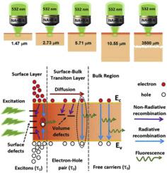
Abstract Carrier transfer is a key process for perovskite-based photoelectric conversion. It has a close relationship with grain boundaries, grain size, and contact layers. Understanding this relationship is of great significance for revealing the inherent characteristics of perovskite materials and for devices optimization. However, the dependence of carrier transfer characteristics (including carrier lifetime and mobility) on thickness is less studied, although which is a key issue for almost all perovskite material devices. Here we find that as the thickness of MAPbBr3 perovskite single crystal (PSC) increases from 1.47 μm to 10.55 μm, the carrier lifetime of MAPbBr3 decreases from 70 ns to 30 ns, and the carrier mobility decreases from 97 cm2 V−1 s−1 to 57 cm2 V−1 s−1, but they become constant in very thick samples. In addition, it was found that as the crystal thickness increased from 1.47 μm to 10.55 μm, the surface layer range gradually increased from 12 nm to 31 nm. The surface recombination velocity and surface defect (trap) density further confirmed that the thin PSC exhibited a small surface layer range. Finally, a three-layer carrier transmission model of PSC is proposed. This research provides guidance for the optimal design of PSC optoelectronic devices.
中文翻译:

MAPbBr3 单晶的厚度相关载流子寿命和迁移率
摘要 载流子转移是钙钛矿基光电转换的关键过程。它与晶界、晶粒尺寸和接触层有密切的关系。理解这种关系对于揭示钙钛矿材料的内在特性和器件优化具有重要意义。然而,载流子转移特性(包括载流子寿命和迁移率)对厚度的依赖性研究较少,尽管这是几乎所有钙钛矿材料器件的关键问题。在这里我们发现,随着 MAPbBr3 钙钛矿单晶 (PSC) 的厚度从 1.47 μm 增加到 10.55 μm,MAPbBr3 的载流子寿命从 70 ns 降低到 30 ns,载流子迁移率从 97 cm2 V−1 s−1 降低到 57 cm2 V−1 s−1,但它们在非常厚的样品中变得恒定。此外,发现随着晶体厚度从 1.47 μm 增加到 10.55 μm,表面层范围逐渐从 12 nm 增加到 31 nm。表面复合速度和表面缺陷(陷阱)密度进一步证实了薄 PSC 表现出小的表面层范围。最后,提出了PSC的三层载波传输模型。该研究为PSC光电器件的优化设计提供了指导。
更新日期:2020-08-01
中文翻译:
MAPbBr3 单晶的厚度相关载流子寿命和迁移率
摘要 载流子转移是钙钛矿基光电转换的关键过程。它与晶界、晶粒尺寸和接触层有密切的关系。理解这种关系对于揭示钙钛矿材料的内在特性和器件优化具有重要意义。然而,载流子转移特性(包括载流子寿命和迁移率)对厚度的依赖性研究较少,尽管这是几乎所有钙钛矿材料器件的关键问题。在这里我们发现,随着 MAPbBr3 钙钛矿单晶 (PSC) 的厚度从 1.47 μm 增加到 10.55 μm,MAPbBr3 的载流子寿命从 70 ns 降低到 30 ns,载流子迁移率从 97 cm2 V−1 s−1 降低到 57 cm2 V−1 s−1,但它们在非常厚的样品中变得恒定。此外,发现随着晶体厚度从 1.47 μm 增加到 10.55 μm,表面层范围逐渐从 12 nm 增加到 31 nm。表面复合速度和表面缺陷(陷阱)密度进一步证实了薄 PSC 表现出小的表面层范围。最后,提出了PSC的三层载波传输模型。该研究为PSC光电器件的优化设计提供了指导。


 京公网安备 11010802027423号