当前位置:
X-MOL 学术
›
Laser Photonics Rev.
›
论文详情
Our official English website, www.x-mol.net, welcomes your
feedback! (Note: you will need to create a separate account there.)
Micro‐Transfer‐Printed III‐V‐on‐Silicon C‐Band Semiconductor Optical Amplifiers
Laser & Photonics Reviews ( IF 9.8 ) Pub Date : 2020-06-08 , DOI: 10.1002/lpor.201900364 Bahawal Haq 1 , Sulakshna Kumari 1 , Kasper Van Gasse 1 , Jing Zhang 1 , Agnieszka Gocalinska 2 , Emanuele Pelucchi 2 , Brian Corbett 2 , Gunther Roelkens 1
Laser & Photonics Reviews ( IF 9.8 ) Pub Date : 2020-06-08 , DOI: 10.1002/lpor.201900364 Bahawal Haq 1 , Sulakshna Kumari 1 , Kasper Van Gasse 1 , Jing Zhang 1 , Agnieszka Gocalinska 2 , Emanuele Pelucchi 2 , Brian Corbett 2 , Gunther Roelkens 1
Affiliation
|
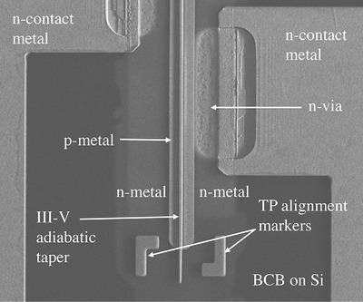
The micro‐transfer‐printing of prefabricated C‐band semiconductor optical amplifiers (SOAs) on a silicon waveguide circuit is reported. The SOAs are 1.35 mm in length and 40 µm in width. Dense arrays of III‐V SOAs are fabricated on the source InP wafer. These can then be micro‐transfer‐printed on the target SOI photonic circuits in a massively parallel fashion. Additionally, this approach allows for greater flexibility in terms of integrating different epitaxial layer structures on the same SOI waveguide circuit. The technique allows integrating SOAs on a complex silicon photonic circuit platform without changing the foundry process‐flow. Two different SOA designs with different optical confinement factor in the quantum wells of the III‐V waveguide are discussed. This allows tuning the small‐signal gain and output saturation power of the SOA. The design with higher optical confinement in the quantum wells has a small‐signal gain of up to 23 dB and an on‐chip saturation power of 9.2 mW at 140 mA bias current and the lower optical confinement factor design has a small‐signal gain of 17 dB and power saturation of 15 mW at 160 mA of bias current.
中文翻译:

微转移印刷的III-V-on-C硅C波段半导体光放大器
报告了预制C波段半导体光放大器(SOA)在硅波导电路上的微转印。SOA的长度为1.35 mm,宽度为40 µm。III-V SOA的密集阵列是在源InP晶圆上制造的。然后可以将它们以大规模并行方式微转移打印在目标SOI光子电路上。另外,这种方法在将不同的外延层结构集成在同一SOI波导电路上方面具有更大的灵活性。该技术允许将SOA集成在复杂的硅光子电路平台上,而无需更改铸造工艺流程。讨论了III‐V波导量子阱中具有不同光学限制因子的两种不同SOA设计。这允许调整SOA的小信号增益和输出饱和功率。
更新日期:2020-06-08
中文翻译:
微转移印刷的III-V-on-C硅C波段半导体光放大器
报告了预制C波段半导体光放大器(SOA)在硅波导电路上的微转印。SOA的长度为1.35 mm,宽度为40 µm。III-V SOA的密集阵列是在源InP晶圆上制造的。然后可以将它们以大规模并行方式微转移打印在目标SOI光子电路上。另外,这种方法在将不同的外延层结构集成在同一SOI波导电路上方面具有更大的灵活性。该技术允许将SOA集成在复杂的硅光子电路平台上,而无需更改铸造工艺流程。讨论了III‐V波导量子阱中具有不同光学限制因子的两种不同SOA设计。这允许调整SOA的小信号增益和输出饱和功率。


 京公网安备 11010802027423号