当前位置:
X-MOL 学术
›
Laser Photonics Rev.
›
论文详情
Our official English website, www.x-mol.net, welcomes your
feedback! (Note: you will need to create a separate account there.)
1.3 µm Quantum Dot‐Distributed Feedback Lasers Directly Grown on (001) Si
Laser & Photonics Reviews ( IF 9.8 ) Pub Date : 2020-06-08 , DOI: 10.1002/lpor.202000037 Yating Wan 1 , Justin C. Norman 2 , Yeyu Tong 3, 4 , M. J. Kennedy 3 , William He 3 , Jenny Selvidge 2 , Chen Shang 2 , Mario Dumont 3 , Aditya Malik 3 , Hon Ki Tsang 4 , Arthur C. Gossard 1, 2, 3 , John E. Bowers 1, 2, 3
Laser & Photonics Reviews ( IF 9.8 ) Pub Date : 2020-06-08 , DOI: 10.1002/lpor.202000037 Yating Wan 1 , Justin C. Norman 2 , Yeyu Tong 3, 4 , M. J. Kennedy 3 , William He 3 , Jenny Selvidge 2 , Chen Shang 2 , Mario Dumont 3 , Aditya Malik 3 , Hon Ki Tsang 4 , Arthur C. Gossard 1, 2, 3 , John E. Bowers 1, 2, 3
Affiliation
|
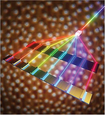
Distributed feedback (DFB) lasers represent a central focus for wavelength‐division‐multiplexing‐based transceivers in metropolitan networks. Here, the first 1.3 µm quantum dot (QD) DFB lasers grown on a complementary metal‐oxide‐semiconductor (CMOS)‐compatible (001) Si substrate are reported. Temperature‐stable, single‐longitudinal‐mode operation is achieved with a side‐mode suppression ratio of more than 50 dB and a threshold current density of 440 A cm−2. A single‐lane rate of 128 Gbit s−1 with a net spectral efficiency of 1.67 bits−1 Hz−1 is demonstrated, with an aggregate total transmission capacity of 640 Gbit s−1 using five channels in the O‐band. Apart from the QD active region growth, the overall fabrication is essentially identical to the commercial process for quantum well (QW) DFB lasers. This provides a process‐compatible path for QD technology into commercial applications previously filled by QW devices. In addition, the capability to grow laser epi across entire CMOS‐compatible (001) Si wafers adds extra benefits of reduced cost, improved heat dissipation, and manufacturing scalability. Through direct epitaxial integration of III–Vs and Si, one can envision a revolution of the photonics industry in the same way that CMOS design and processing revolutionize the microelectronics industry. This is discussed from a system perspective for on‐chip optical interconnects.
中文翻译:

直接在(001)Si上生长的1.3 µm量子点分布反馈激光器
分布式反馈(DFB)激光器代表了城域网中基于波分复用的收发器的重点。此处报道了在互补金属氧化物半导体(CMOS)兼容(001)硅衬底上生长的第一批1.3 µm量子点(QD)DFB激光器。通过超过50 dB的旁模抑制比和440 A cm -2的阈值电流密度,实现了温度稳定的单纵向模式操作。单通道速率为128 Gbit s -1,净频谱效率为1.67 bit -1 Hz -1,总传输容量总计为640 Gbit s -1在O波段使用五个通道。除了QD有源区的增长以外,整个制造过程基本上与量子阱(QW)DFB激光器的商业化过程相同。这为QD技术进入先前由QW设备填充的商业应用提供了过程兼容的途径。此外,在整个CMOS兼容(001)硅晶片上生长激光落射的能力还增加了降低成本,改善散热和制造可扩展性的额外优势。通过III-Vs和Si的直接外延集成,可以像CMOS设计和处理技术彻底改变微电子工业一样,预见光子产业的革命。从系统角度讨论了片上光学互连。
更新日期:2020-06-08
中文翻译:
直接在(001)Si上生长的1.3 µm量子点分布反馈激光器
分布式反馈(DFB)激光器代表了城域网中基于波分复用的收发器的重点。此处报道了在互补金属氧化物半导体(CMOS)兼容(001)硅衬底上生长的第一批1.3 µm量子点(QD)DFB激光器。通过超过50 dB的旁模抑制比和440 A cm -2的阈值电流密度,实现了温度稳定的单纵向模式操作。单通道速率为128 Gbit s -1,净频谱效率为1.67 bit -1 Hz -1,总传输容量总计为640 Gbit s -1在O波段使用五个通道。除了QD有源区的增长以外,整个制造过程基本上与量子阱(QW)DFB激光器的商业化过程相同。这为QD技术进入先前由QW设备填充的商业应用提供了过程兼容的途径。此外,在整个CMOS兼容(001)硅晶片上生长激光落射的能力还增加了降低成本,改善散热和制造可扩展性的额外优势。通过III-Vs和Si的直接外延集成,可以像CMOS设计和处理技术彻底改变微电子工业一样,预见光子产业的革命。从系统角度讨论了片上光学互连。


 京公网安备 11010802027423号