当前位置:
X-MOL 学术
›
Phys. Status Solidi. Rapid Res. Lett.
›
论文详情
Our official English website, www.x-mol.net, welcomes your
feedback! (Note: you will need to create a separate account there.)
Vanishing Hysteresis in Carbon Nanotube Transistors Embedded in Boron Nitride/Polytetrafluoroethylene Heterolayers
Physica Status Solidi-Rapid Research Letters ( IF 2.5 ) Pub Date : 2020-06-16 , DOI: 10.1002/pssr.202000193 Sandeep Kumar 1, 2 , Daghan Dagli 1, 2 , Simone Dehm 1 , Chittaranjan Das 3 , Li Wei 4 , Yuan Chen 4 , Frank Hennrich 5 , Ralph Krupke 1, 2, 5
Physica Status Solidi-Rapid Research Letters ( IF 2.5 ) Pub Date : 2020-06-16 , DOI: 10.1002/pssr.202000193 Sandeep Kumar 1, 2 , Daghan Dagli 1, 2 , Simone Dehm 1 , Chittaranjan Das 3 , Li Wei 4 , Yuan Chen 4 , Frank Hennrich 5 , Ralph Krupke 1, 2, 5
Affiliation
|
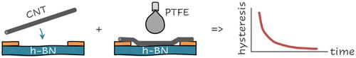
Carbon nanotube field‐effect transistors fabricated on silicon wafers with thermal oxide often suffer from large gate‐voltage hysteresis, induced by charge trapping sites in oxides, surface hydroxyl groups, and the presence of water molecules. Surface functionalization and passivation, as well as vacuum annealing and reduced operating temperature, have shown to diminish or even eliminate hysteresis. Herein, the fabrication of nearly hysteresis‐free transistors on Si/SiO2 by embedding carbon nanotubes and the connecting electrodes in a hexagonal boron nitride (h‐BN) bottom layer and a polytetrafluoroethylene (PTFE) top layer is demonstrated. The conditions at which catalyst‐free synthesis of h‐BN on SiO2/Si with borazine is obtained, and the subsequent liquid‐phase deposition of PTFE, are discussed. Device transfer curves are measured before and after PTFE deposition. It is found that the hysteresis is reduced after PTFE deposition, but vanishes only after a waiting period of several days. Simultaneously, the on‐state current increases with time. The results give evidence for the absence of trap states in h‐BN/PTFE heterolayers and a high breakthrough field strength in those wafer‐scalable materials.
中文翻译:

氮化硼/聚四氟乙烯异质层中嵌入的碳纳米管晶体管的磁滞消失
在带有热氧化物的硅晶片上制造的碳纳米管场效应晶体管通常会遭受较大的栅极电压滞后现象,这是由氧化物中的电荷俘获位点,表面羟基和水分子的存在引起的。表面功能化和钝化以及真空退火和降低的工作温度已显示出可以减少甚至消除滞后现象。在此,说明了通过将碳纳米管和连接电极嵌入六方氮化硼(h-BN)底层和聚四氟乙烯(PTFE)顶层中,在Si / SiO 2上制造几乎没有磁滞的晶体管。在SiO 2上无催化剂合成h-BN的条件获得了含硼嗪的/ Si,并讨论了随后的PTFE液相沉积。在PTFE沉积之前和之后测量器件转移曲线。发现在PTFE沉积之后,磁滞减小,但是仅在等待几天后消失。同时,导通电流随时间增加。结果提供了证据,证明在h‐BN / PTFE杂层中不存在陷阱态,而那些可晶片缩放的材料具有很高的突破场强。
更新日期:2020-06-16
中文翻译:
氮化硼/聚四氟乙烯异质层中嵌入的碳纳米管晶体管的磁滞消失
在带有热氧化物的硅晶片上制造的碳纳米管场效应晶体管通常会遭受较大的栅极电压滞后现象,这是由氧化物中的电荷俘获位点,表面羟基和水分子的存在引起的。表面功能化和钝化以及真空退火和降低的工作温度已显示出可以减少甚至消除滞后现象。在此,说明了通过将碳纳米管和连接电极嵌入六方氮化硼(h-BN)底层和聚四氟乙烯(PTFE)顶层中,在Si / SiO 2上制造几乎没有磁滞的晶体管。在SiO 2上无催化剂合成h-BN的条件获得了含硼嗪的/ Si,并讨论了随后的PTFE液相沉积。在PTFE沉积之前和之后测量器件转移曲线。发现在PTFE沉积之后,磁滞减小,但是仅在等待几天后消失。同时,导通电流随时间增加。结果提供了证据,证明在h‐BN / PTFE杂层中不存在陷阱态,而那些可晶片缩放的材料具有很高的突破场强。


 京公网安备 11010802027423号