当前位置:
X-MOL 学术
›
Acc. Chem. Res.
›
论文详情
Our official English website, www.x-mol.net, welcomes your
feedback! (Note: you will need to create a separate account there.)
Mechanisms of Thermal Atomic Layer Etching.
Accounts of Chemical Research ( IF 16.4 ) Pub Date : 2020-06-01 , DOI: 10.1021/acs.accounts.0c00084 Steven M George 1
Accounts of Chemical Research ( IF 16.4 ) Pub Date : 2020-06-01 , DOI: 10.1021/acs.accounts.0c00084 Steven M George 1
Affiliation
|
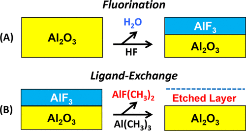
Atomic layer control of semiconductor processing is needed as critical dimensions are progressively reduced below the 10 nm scale. Atomic layer deposition (ALD) methods are meeting this challenge and produce conformal thin film growth on high aspect ratio features. Atomic layer etching (ALE) techniques are also required that can remove material with atomic layer precision. ALE processes are defined using sequential, self-limiting reactions based on surface modification and volatile release. Plasma ALE methods employ energetic ion or neutral species to release the modified material anisotropically using sputtering. In contrast, thermal ALE processes utilize gas species to release the modified material isotropically using thermal reactions. Thermal ALE can be viewed as the “reverse of ALD”.
中文翻译:

热原子层蚀刻的机制。
由于关键尺寸逐渐减小到10 nm以下,因此需要半导体工艺的原子层控制。原子层沉积(ALD)方法正迎接这一挑战,并在高深宽比特征上产生了保形的薄膜生长。还需要能够以原子层精度去除材料的原子层蚀刻(ALE)技术。使用基于表面修饰和挥发物释放的顺序自限反应定义ALE过程。等离子ALE方法采用高能离子或中性物质,通过溅射各向异性地释放改性材料。相比之下,热ALE工艺利用气体种类通过热反应各向同性地释放改性材料。热ALE可以看作是“ ALD的逆向”。
更新日期:2020-06-01
中文翻译:
热原子层蚀刻的机制。
由于关键尺寸逐渐减小到10 nm以下,因此需要半导体工艺的原子层控制。原子层沉积(ALD)方法正迎接这一挑战,并在高深宽比特征上产生了保形的薄膜生长。还需要能够以原子层精度去除材料的原子层蚀刻(ALE)技术。使用基于表面修饰和挥发物释放的顺序自限反应定义ALE过程。等离子ALE方法采用高能离子或中性物质,通过溅射各向异性地释放改性材料。相比之下,热ALE工艺利用气体种类通过热反应各向同性地释放改性材料。热ALE可以看作是“ ALD的逆向”。


 京公网安备 11010802027423号