Our official English website, www.x-mol.net, welcomes your
feedback! (Note: you will need to create a separate account there.)
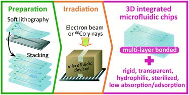
A simple method for production of hydrophilic, rigid, and sterilized multi-layer 3D integrated polydimethylsiloxane microfluidic chips.
Lab on a Chip ( IF 6.1 ) Pub Date : 2020-05-28 , DOI: 10.1039/d0lc00316f Tomoko Gowa Oyama 1 , Kotaro Oyama , Mitsumasa Taguchi
Lab on a Chip ( IF 6.1 ) Pub Date : 2020-05-28 , DOI: 10.1039/d0lc00316f Tomoko Gowa Oyama 1 , Kotaro Oyama , Mitsumasa Taguchi
Affiliation
|
Polydimethylsiloxane (PDMS) has many desirable features for microfluidics applications, particularly in diagnostics and pharmaceuticals, but its hydrophobicity and the lack of a practical method for bonding PDMS layers limit its use. Moreover, the flexibility of PDMS causes unwanted deformation during use in some applications. Here, we report a simple method for solving these problems simultaneously using an electron beam (EB) or γ-rays, which are commonly used for sterilizing medical products. Simply by applying EB or γ-ray irradiation to stacked PDMS layers, we can not only bond the interfaces between the layers by forming Si–O–Si covalent bonds but also achieve long-lasting hydrophilization and sterilization of the internal microchannels and chambers, prevent nonspecific adsorption and absorption of hydrophobic small molecules, and enhance the mechanical strength of the material by converting bulk PDMS into a Si–Ox-rich (where x is 3 or 4) structure though crosslinking. Unlike the one-at-a-time plasma process, EBs and γ-rays can penetrate through many stacked layers of PDMS sealed in their final package, enabling batch modification and bonding. The method requires no chemical crosslinkers, adhesive agents, or fillers; hence, it does not undermine the advantages of PDMS such as ease of molding in soft lithography, biocompatibility, and optical transparency. Furthermore, bonding is achieved with high-throughput yield because it occurs after re-adjustable alignment. We demonstrate that this method is applicable in the mass production of 3D integrated PDMS microfluidic chips with some glass-like properties as well as for 3D structures with complex shapes that are difficult to fabricate with plastic or glass.
中文翻译:

一种生产亲水,刚性和灭菌的多层3D集成聚二甲基硅氧烷微流体芯片的简单方法。
聚二甲基硅氧烷(PDMS)在微流体应用中具有许多理想的功能,特别是在诊断和制药领域,但是其疏水性和粘合PDMS层的实际方法的缺乏限制了它的使用。此外,PDMS的灵活性在某些应用中会导致不必要的变形。在这里,我们报告了一种简单的方法,该方法可以使用通常用于医疗产品消毒的电子束(EB)或γ射线同时解决这些问题。只需通过对堆叠的PDMS层进行EB或γ射线辐照,我们不仅可以通过形成Si–O–Si共价键来键合各层之间的界面,还可以实现持久的亲水化和内部微通道和腔室的灭菌,防止疏水性小分子的非特异性吸附和吸收,X富含(其中X是3或4)结构虽然交联。与一次性等离子体处理不同,电子束和γ射线可以穿透密封在其最终包装中的PDMS的许多堆叠层,从而实现批处理修改和粘合。该方法不需要化学交联剂,粘合剂或填料。因此,它不会损害PDMS的优势,例如易于在软光刻中成型,生物相容性和光学透明性。此外,以高通量产率实现键合,因为它在重新可调的对准之后发生。我们证明该方法适用于大规模生产具有某些玻璃样特性的3D集成PDMS微流体芯片,以及适用于难以用塑料或玻璃制造的形状复杂的3D结构。
更新日期:2020-06-30
中文翻译:
一种生产亲水,刚性和灭菌的多层3D集成聚二甲基硅氧烷微流体芯片的简单方法。
聚二甲基硅氧烷(PDMS)在微流体应用中具有许多理想的功能,特别是在诊断和制药领域,但是其疏水性和粘合PDMS层的实际方法的缺乏限制了它的使用。此外,PDMS的灵活性在某些应用中会导致不必要的变形。在这里,我们报告了一种简单的方法,该方法可以使用通常用于医疗产品消毒的电子束(EB)或γ射线同时解决这些问题。只需通过对堆叠的PDMS层进行EB或γ射线辐照,我们不仅可以通过形成Si–O–Si共价键来键合各层之间的界面,还可以实现持久的亲水化和内部微通道和腔室的灭菌,防止疏水性小分子的非特异性吸附和吸收,X富含(其中X是3或4)结构虽然交联。与一次性等离子体处理不同,电子束和γ射线可以穿透密封在其最终包装中的PDMS的许多堆叠层,从而实现批处理修改和粘合。该方法不需要化学交联剂,粘合剂或填料。因此,它不会损害PDMS的优势,例如易于在软光刻中成型,生物相容性和光学透明性。此外,以高通量产率实现键合,因为它在重新可调的对准之后发生。我们证明该方法适用于大规模生产具有某些玻璃样特性的3D集成PDMS微流体芯片,以及适用于难以用塑料或玻璃制造的形状复杂的3D结构。


 京公网安备 11010802027423号