当前位置:
X-MOL 学术
›
Adv. Electron. Mater.
›
论文详情
Our official English website, www.x-mol.net, welcomes your
feedback! (Note: you will need to create a separate account there.)
Field Emission in Ultrathin PdSe2 Back‐Gated Transistors
Advanced Electronic Materials ( IF 5.3 ) Pub Date : 2020-05-20 , DOI: 10.1002/aelm.202000094 Antonio Di Bartolomeo 1, 2 , Aniello Pelella 1, 2 , Francesca Urban 1, 2 , Alessandro Grillo 1, 2 , Laura Iemmo 1, 2 , Maurizio Passacantando 3 , Xiaowei Liu 4 , Filippo Giubileo 2
Advanced Electronic Materials ( IF 5.3 ) Pub Date : 2020-05-20 , DOI: 10.1002/aelm.202000094 Antonio Di Bartolomeo 1, 2 , Aniello Pelella 1, 2 , Francesca Urban 1, 2 , Alessandro Grillo 1, 2 , Laura Iemmo 1, 2 , Maurizio Passacantando 3 , Xiaowei Liu 4 , Filippo Giubileo 2
Affiliation
|
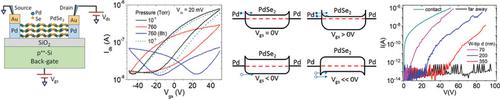
This study deals with the electrical transport in back‐gate field‐effect transistors with ultrathin palladium diselenide (PdSe2) channels. The devices are normally‐on and exhibit dominant n‐type conduction at low pressure. The electron conduction of PdSe2 nanosheets, combined with the sharp edge and the work function decreasing with the number of layers, opens up new applications in vacuum electronics. This work is the first experimental demonstration of field emission current from few‐layer PdSe2 and extends the plethora of applications of this recently isolated pentagonal layered material. Field‐emission from PdSe2 nanosheets is obtained with a turn‐on field below 100 V µm−1 and attains currents up to the µA.
中文翻译:

超薄PdSe2背栅晶体管的场发射
本研究涉及具有超薄二硒化钯(PdSe 2)通道的背栅场效应晶体管的电传输。器件常开,在低压下表现出主要的n型导通。PdSe 2纳米片的电子传导,加上锋利的边缘和功函数随着层数的减少而下降,为真空电子学开辟了新的应用领域。这项工作是几层PdSe 2场发射电流的第一个实验演示,扩展了这种最近隔离的五边形层状材料的大量应用。PdSe 2纳米片的场发射是在低于100 V µm -1的开启场下获得的 并获得高达µA的电流。
更新日期:2020-07-13
中文翻译:
超薄PdSe2背栅晶体管的场发射
本研究涉及具有超薄二硒化钯(PdSe 2)通道的背栅场效应晶体管的电传输。器件常开,在低压下表现出主要的n型导通。PdSe 2纳米片的电子传导,加上锋利的边缘和功函数随着层数的减少而下降,为真空电子学开辟了新的应用领域。这项工作是几层PdSe 2场发射电流的第一个实验演示,扩展了这种最近隔离的五边形层状材料的大量应用。PdSe 2纳米片的场发射是在低于100 V µm -1的开启场下获得的 并获得高达µA的电流。


 京公网安备 11010802027423号