当前位置:
X-MOL 学术
›
Int. J. Circ. Theory Appl.
›
论文详情
Our official English website, www.x-mol.net, welcomes your
feedback! (Note: you will need to create a separate account there.)
FinFET‐based power‐efficient, low leakage, and area‐efficient DWT lifting architecture using power gating and reversible logic
International Journal of Circuit Theory and Applications ( IF 1.8 ) Pub Date : 2020-05-16 , DOI: 10.1002/cta.2794 Kesavan Subannan Palanisamy 1 , Rajeswari Ramachandran 2
International Journal of Circuit Theory and Applications ( IF 1.8 ) Pub Date : 2020-05-16 , DOI: 10.1002/cta.2794 Kesavan Subannan Palanisamy 1 , Rajeswari Ramachandran 2
Affiliation
|
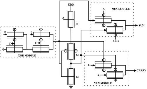
For ultra‐low‐power applications, the computing components are smaller in size and consume less energy. In nonstationary signal analysis, the transformation plays an important role. Out of different transformation techniques, the most famous and dominant architecture is the discrete wavelet transform. The building block of the architecture should be optimized by all parameters. In this paper, the optimization was done on the power reduction and leakage current reduction. A new FinFET‐based lifting‐based wavelet architecture was proposed. Power gating and reversible logic methodology are proposed for the FinFET‐based transform to reduce the dynamic power by about 30%. The proposed FinFET‐based processing elements were utilized in the various blocks of the lifting‐based DWT architecture. The implementation was done in 32‐nm CMOS and FinFET technology. From the results, it has been investigated that the FinFET‐based circuits are efficient when compared with CMOS technology. This is due to the second‐order effects happening in CMOS circuits below 45 nm. The proposed design consumes less area and low leakage current and power when compared with the CMOS technology. Future trends of using multigate devices below 14 nm technology are presented finally.
中文翻译:

使用电源门控和可逆逻辑的基于FinFET的节能,低泄漏和面积有效的DWT提升架构
对于超低功耗应用,计算组件尺寸更小,能耗更低。在非平稳信号分析中,转换起着重要作用。在不同的变换技术中,最著名和占主导地位的体系结构是离散小波变换。应该通过所有参数优化体系结构的构建块。本文对功耗降低和漏电流降低进行了优化。提出了一种新的基于FinFET的基于提升的小波架构。针对基于FinFET的变换,提出了功率门控和可逆逻辑方法,以将动态功率降低约30%。提议的基于FinFET的处理元件被用于基于提升的DWT体系结构的各个模块中。该实现是在32nm CMOS和FinFET技术中完成的。从结果可以看出,与CMOS技术相比,基于FinFET的电路是高效的。这是由于在45 nm以下的CMOS电路中发生了二次效应。与CMOS技术相比,拟议的设计消耗的面积较小,漏电流和功耗低。最后介绍了使用低于14 nm技术的多栅极器件的未来趋势。
更新日期:2020-05-16
中文翻译:
使用电源门控和可逆逻辑的基于FinFET的节能,低泄漏和面积有效的DWT提升架构
对于超低功耗应用,计算组件尺寸更小,能耗更低。在非平稳信号分析中,转换起着重要作用。在不同的变换技术中,最著名和占主导地位的体系结构是离散小波变换。应该通过所有参数优化体系结构的构建块。本文对功耗降低和漏电流降低进行了优化。提出了一种新的基于FinFET的基于提升的小波架构。针对基于FinFET的变换,提出了功率门控和可逆逻辑方法,以将动态功率降低约30%。提议的基于FinFET的处理元件被用于基于提升的DWT体系结构的各个模块中。该实现是在32nm CMOS和FinFET技术中完成的。从结果可以看出,与CMOS技术相比,基于FinFET的电路是高效的。这是由于在45 nm以下的CMOS电路中发生了二次效应。与CMOS技术相比,拟议的设计消耗的面积较小,漏电流和功耗低。最后介绍了使用低于14 nm技术的多栅极器件的未来趋势。


 京公网安备 11010802027423号