当前位置:
X-MOL 学术
›
Mater. Today Phys.
›
论文详情
Our official English website, www.x-mol.net, welcomes your feedback! (Note: you will need to create a separate account there.)
Low Temperature Defect Passivation Technology for Semiconductor Electronic Devices - Supercritical Fluids Treatment Process
Materials Today Physics ( IF 11.5 ) Pub Date : 2020-08-01 , DOI: 10.1016/j.mtphys.2020.100225 T.-C. Chang , P.-H. Chen , C.-Y. Lin , C.-C. Shih
Materials Today Physics ( IF 11.5 ) Pub Date : 2020-08-01 , DOI: 10.1016/j.mtphys.2020.100225 T.-C. Chang , P.-H. Chen , C.-Y. Lin , C.-C. Shih
|
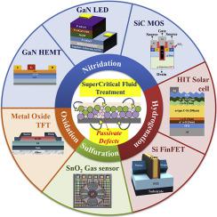
Abstract Currently, defects existing in materials and at the interface are the main bottlenecks limiting the manufacture of high-performance electron devices, especially semiconductor devices where the performance and reliability are affected by these defects. Therefore, high temperature annealing (HTA) is often applied to passivate defects, though it raises additional issues in the device fabrication process, such as heat budget and impurity diffusion. In this article, we propose a passivation technique induced by a supercritical fluid (SCF) treatment at relative low temperatures and test it for use in various devices. The SCF treatment is equipped with both high permeability and solubility to introduce reactive substances which act to passivate defects and further enhance device performance without altering the device material or making major changes to the fabrication process. The experimental results prove that this technique can be applied to the AlGaN-based ultraviolet C light-emitting diode to increase the band-to-band emission spectrum of 280 nm, as compared with the 360 nm emission spectrum of defects. The electrical characteristics of the GaN-based high electron mobility transistor including on/off currents, trans-conductance (Gm), and current collapse were also improved. Such a SCF treatment can also be applied to Si-based fin field effect transistors to increase the Gm and mobility because of reduction of defect concentration. This SCF treatment was also applied to a current-production heterojunction with intrinsic thin layer solar cell to improve the efficiency from 18.2% to 19.5%. Using this SCF treatment on InGaZnO thin film transistors results in effective suppression of the VTH shift, which proves the defects in the gate insulator have been eliminated. The SCF treatment has also been applied to a SnO2 gas sensor to increase the selectivity and endurance to humidity because of the passivation of vacancies. These all confirm that this SCF treatment's passivation capability can be applied to various electron devices. In addition, this SCF treatment has the advantages of being performed at low-temperature in a non-destructive process in a batch treatment with high selectivity, which provides the semiconductor industry a method to solve the manufacturing bottleneck in advanced electron devices.
中文翻译:

半导体电子器件低温缺陷钝化技术-超临界流体处理工艺
摘要 目前,材料中和界面处存在的缺陷是制约高性能电子器件尤其是半导体器件制造的主要瓶颈,这些缺陷会影响其性能和可靠性。因此,高温退火 (HTA) 通常用于钝化缺陷,尽管它会在器件制造过程中引发其他问题,例如热预算和杂质扩散。在本文中,我们提出了一种在相对低温下由超临界流体 (SCF) 处理引起的钝化技术,并对其在各种设备中的使用进行了测试。SCF 处理具有高渗透性和溶解性,可引入活性物质,这些物质可钝化缺陷并进一步增强器件性能,而无需改变器件材料或对制造工艺进行重大改变。实验结果证明,该技术可应用于AlGaN基紫外C发光二极管,与缺陷的360nm发射光谱相比,增加了280nm的带间发射光谱。GaN 基高电子迁移率晶体管的电气特性包括开/关电流、跨导 (Gm) 和电流崩塌也得到了改善。这种 SCF 处理也可以应用于 Si 基鳍式场效应晶体管,以增加 Gm 和迁移率,因为减少了缺陷浓度。这种 SCF 处理还应用于当前生产的带有本征薄层太阳能电池的异质结,以将效率从 18.2% 提高到 19.5%。在 InGaZnO 薄膜晶体管上使用这种 SCF 处理可有效抑制 VTH 偏移,这证明栅极绝缘体中的缺陷已被消除。由于空位钝化,SCF 处理也已应用于 SnO2 气体传感器,以提高选择性和对湿度的耐受性。这些都证实了这种SCF处理的钝化能力可以应用于各种电子器件。此外,这种SCF处理的优点是可以在低温下以非破坏性的方式进行批量处理,具有高选择性,
更新日期:2020-08-01
中文翻译:
半导体电子器件低温缺陷钝化技术-超临界流体处理工艺
摘要 目前,材料中和界面处存在的缺陷是制约高性能电子器件尤其是半导体器件制造的主要瓶颈,这些缺陷会影响其性能和可靠性。因此,高温退火 (HTA) 通常用于钝化缺陷,尽管它会在器件制造过程中引发其他问题,例如热预算和杂质扩散。在本文中,我们提出了一种在相对低温下由超临界流体 (SCF) 处理引起的钝化技术,并对其在各种设备中的使用进行了测试。SCF 处理具有高渗透性和溶解性,可引入活性物质,这些物质可钝化缺陷并进一步增强器件性能,而无需改变器件材料或对制造工艺进行重大改变。实验结果证明,该技术可应用于AlGaN基紫外C发光二极管,与缺陷的360nm发射光谱相比,增加了280nm的带间发射光谱。GaN 基高电子迁移率晶体管的电气特性包括开/关电流、跨导 (Gm) 和电流崩塌也得到了改善。这种 SCF 处理也可以应用于 Si 基鳍式场效应晶体管,以增加 Gm 和迁移率,因为减少了缺陷浓度。这种 SCF 处理还应用于当前生产的带有本征薄层太阳能电池的异质结,以将效率从 18.2% 提高到 19.5%。在 InGaZnO 薄膜晶体管上使用这种 SCF 处理可有效抑制 VTH 偏移,这证明栅极绝缘体中的缺陷已被消除。由于空位钝化,SCF 处理也已应用于 SnO2 气体传感器,以提高选择性和对湿度的耐受性。这些都证实了这种SCF处理的钝化能力可以应用于各种电子器件。此外,这种SCF处理的优点是可以在低温下以非破坏性的方式进行批量处理,具有高选择性,


 京公网安备 11010802027423号