当前位置:
X-MOL 学术
›
Chem. Mater.
›
论文详情
Our official English website, www.x-mol.net, welcomes your
feedback! (Note: you will need to create a separate account there.)
Area-Selective Deposition: Fundamentals, Applications, and Future Outlook
Chemistry of Materials ( IF 7.2 ) Pub Date : 2020-05-14 , DOI: 10.1021/acs.chemmater.0c00722 Gregory N. Parsons 1 , Robert D. Clark 2
Chemistry of Materials ( IF 7.2 ) Pub Date : 2020-05-14 , DOI: 10.1021/acs.chemmater.0c00722 Gregory N. Parsons 1 , Robert D. Clark 2
Affiliation
|
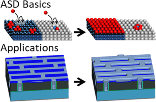
This review provides an overview of area-selective thin film deposition (ASD) with a primary focus on vapor-phase thin film formation via chemical vapor deposition (CVD) and atomic layer deposition (ALD). Area-selective deposition has been successfully implemented in microelectronic processes, but most approaches to date rely on high-temperature reactions to achieve the desired substrate sensitivity. Continued size and performance scaling of microelectronics, as well as new materials, patterning methods, and device fabrication schemes are seeking solutions for new low-temperature (<400 °C) ASD methods for dielectrics, metals, and organic thin films. To provide an overview of the ASD field, this article critically reviews key challenges that must be overcome for ASD to be successful in microelectronics and other fields, including descriptions of current process application needs. We provide an overview of basic mechanisms in film nucleation during CVD and ALD and summarize current known ASD approaches for semiconductors, metals, dielectrics, and organic materials. For a few key materials, selectivity is quantitatively compared for different reaction precursors, giving important insight into needs for favorable reactant and reaction design. We summarize current limitations of ASD and future opportunities that could be achieved using advanced bottom-up atomic scale processes.
中文翻译:

区域选择性沉积:基本原理,应用和未来展望
这篇综述提供了区域选择性薄膜沉积(ASD)的概述,主要侧重于通过化学气相沉积(CVD)和原子层沉积(ALD)形成气相薄膜。区域选择性沉积已在微电子工艺中成功实现,但是迄今为止,大多数方法都依赖于高温反应来实现所需的基板灵敏度。微电子技术的持续尺寸和性能缩放以及新材料,图案化方法和器件制造方案正在寻求针对电介质,金属和有机薄膜的新型低温(<400°C)ASD方法的解决方案。为了概述ASD领域,本文严格审查了ASD在微电子学和其他领域取得成功所必须克服的关键挑战,包括当前流程应用程序需求的描述。我们概述了CVD和ALD过程中成膜的基本机理,并总结了当前已知的用于半导体,金属,电介质和有机材料的ASD方法。对于一些关键材料,定量比较了不同反应前体的选择性,从而深入了解了对有利的反应物和反应设计的需求。我们总结了ASD的当前局限性以及使用先进的自下而上的原子尺度工艺可以实现的未来机会。定量比较了不同反应前体的选择性,从而深入了解了对有利的反应物和反应设计的需求。我们总结了ASD的当前局限性以及使用先进的自下而上的原子尺度工艺可以实现的未来机会。定量比较了不同反应前体的选择性,从而深入了解了对有利的反应物和反应设计的需求。我们总结了ASD的当前局限性以及使用先进的自下而上的原子尺度工艺可以实现的未来机会。
更新日期:2020-06-23
中文翻译:
区域选择性沉积:基本原理,应用和未来展望
这篇综述提供了区域选择性薄膜沉积(ASD)的概述,主要侧重于通过化学气相沉积(CVD)和原子层沉积(ALD)形成气相薄膜。区域选择性沉积已在微电子工艺中成功实现,但是迄今为止,大多数方法都依赖于高温反应来实现所需的基板灵敏度。微电子技术的持续尺寸和性能缩放以及新材料,图案化方法和器件制造方案正在寻求针对电介质,金属和有机薄膜的新型低温(<400°C)ASD方法的解决方案。为了概述ASD领域,本文严格审查了ASD在微电子学和其他领域取得成功所必须克服的关键挑战,包括当前流程应用程序需求的描述。我们概述了CVD和ALD过程中成膜的基本机理,并总结了当前已知的用于半导体,金属,电介质和有机材料的ASD方法。对于一些关键材料,定量比较了不同反应前体的选择性,从而深入了解了对有利的反应物和反应设计的需求。我们总结了ASD的当前局限性以及使用先进的自下而上的原子尺度工艺可以实现的未来机会。定量比较了不同反应前体的选择性,从而深入了解了对有利的反应物和反应设计的需求。我们总结了ASD的当前局限性以及使用先进的自下而上的原子尺度工艺可以实现的未来机会。定量比较了不同反应前体的选择性,从而深入了解了对有利的反应物和反应设计的需求。我们总结了ASD的当前局限性以及使用先进的自下而上的原子尺度工艺可以实现的未来机会。


 京公网安备 11010802027423号