当前位置:
X-MOL 学术
›
Small Methods
›
论文详情
Our official English website, www.x-mol.net, welcomes your
feedback! (Note: you will need to create a separate account there.)
Wafer‐Scale Fabrication of Nanopore Devices for Single‐Molecule DNA Biosensing using MoS2
Small Methods ( IF 10.7 ) Pub Date : 2020-05-11 , DOI: 10.1002/smtd.202000072 Mukeshchand Thakur 1 , Michal Macha 1 , Andrey Chernev 1 , Michael Graf 1 , Martina Lihter 1 , Jochem Deen 1 , Mukesh Tripathi 2 , Andras Kis 2 , Aleksandra Radenovic 1
Small Methods ( IF 10.7 ) Pub Date : 2020-05-11 , DOI: 10.1002/smtd.202000072 Mukeshchand Thakur 1 , Michal Macha 1 , Andrey Chernev 1 , Michael Graf 1 , Martina Lihter 1 , Jochem Deen 1 , Mukesh Tripathi 2 , Andras Kis 2 , Aleksandra Radenovic 1
Affiliation
|
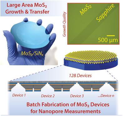
Atomically thin (2D) nanoporous membranes are an excellent platform for a broad scope of academic research. Their thickness and intrinsic ion selectivity (demonstrated for example in molybdenum disulfide‐MoS2) make them particularly attractive for single‐molecule biosensing experiments and osmotic energy harvesting membranes. Currently, one of the major challenges associated with the research progress and industrial development of 2D nanopore membrane devices is small‐scale thin‐film growth and small‐area transfer methods. To address these issues, a large‐area protocol including a wafer‐scale monolayer MoS2 synthesis, Si/SiNx substrate fabrication and wafer‐scale material transfer are demonstrated. First, the 7.62 cm wafer‐scale MOCVD growth yielding homogenous monolayer MoS2 films are introduced. Second, a large number of devices are fabricated in one batch by employing the wafer‐scale thin‐film transfer method with high transfer efficiency (>70% device yield). The growth, the transfer quality and cleanliness are investigated using transmission electron microscopy, atomic force microscopy and Raman spectroscopy. Finally, the applicability and robustness of the large‐area protocol is demonstrated by performing a set of double‐stranded DNA translocation experiments through as‐fabricated MoS2 nanopore devices. It is believed that the shown approach will pave the way toward wafer‐scale, high‐throughput use of 2D nanopores in various applications.
中文翻译:

MoS2用于单分子DNA生物传感的纳米孔器件的晶圆级制备。
原子薄(2D)纳米多孔膜是广泛学术研究的绝佳平台。它们的厚度和固有离子选择性(例如在二硫化钼-MoS 2中证明)使它们对单分子生物传感实验和渗透能收集膜特别有吸引力。当前,与二维纳米孔膜器件的研究进展和产业发展相关的主要挑战之一是小规模的薄膜生长和小面积转移方法。为了解决这些问题,采用了包括晶圆级单层MoS 2合成,Si / SiN x的大面积协议演示了基板制造和晶圆级材料转移。首先,介绍了7.62 cm晶圆级MOCVD生长产生均匀的单层MoS 2膜的方法。其次,采用晶圆级薄膜转移方法以高转移效率(> 70%的设备良率)批量生产大量设备。使用透射电子显微镜,原子力显微镜和拉曼光谱对生长,转移质量和清洁度进行了研究。最后,通过使用预制的MoS 2进行一组双链DNA易位实验,证明了大面积协议的适用性和鲁棒性。纳米孔设备。据信,所示方法将为在各种应用中晶圆级,高通量使用二维纳米孔铺平道路。
更新日期:2020-05-11
中文翻译:
MoS2用于单分子DNA生物传感的纳米孔器件的晶圆级制备。
原子薄(2D)纳米多孔膜是广泛学术研究的绝佳平台。它们的厚度和固有离子选择性(例如在二硫化钼-MoS 2中证明)使它们对单分子生物传感实验和渗透能收集膜特别有吸引力。当前,与二维纳米孔膜器件的研究进展和产业发展相关的主要挑战之一是小规模的薄膜生长和小面积转移方法。为了解决这些问题,采用了包括晶圆级单层MoS 2合成,Si / SiN x的大面积协议演示了基板制造和晶圆级材料转移。首先,介绍了7.62 cm晶圆级MOCVD生长产生均匀的单层MoS 2膜的方法。其次,采用晶圆级薄膜转移方法以高转移效率(> 70%的设备良率)批量生产大量设备。使用透射电子显微镜,原子力显微镜和拉曼光谱对生长,转移质量和清洁度进行了研究。最后,通过使用预制的MoS 2进行一组双链DNA易位实验,证明了大面积协议的适用性和鲁棒性。纳米孔设备。据信,所示方法将为在各种应用中晶圆级,高通量使用二维纳米孔铺平道路。


 京公网安备 11010802027423号