当前位置:
X-MOL 学术
›
Micro Nanostruct.
›
论文详情
Our official English website, www.x-mol.net, welcomes your
feedback! (Note: you will need to create a separate account there.)
Molybdenum disulfide thin films fabrication from multi-phase molybdenum oxide using magnetron sputtering and CVD systems together
Micro and Nanostructures ( IF 2.7 ) Pub Date : 2020-07-01 , DOI: 10.1016/j.spmi.2020.106555 Ayşe Karataş , Mücahit Yılmaz
Micro and Nanostructures ( IF 2.7 ) Pub Date : 2020-07-01 , DOI: 10.1016/j.spmi.2020.106555 Ayşe Karataş , Mücahit Yılmaz
|
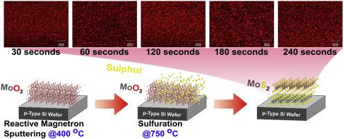
Abstract Molybdenum disulfide (MoS2) is a layered 2D semiconducting material with a tunable bandgap and a promising materials for next generation optoelectronics applications. In this study, the characterization of large-scale MoS2 films obtained by sulfurization of Mo–O films grown in different thicknesses with reactive magnetron sputtering method at 400 °C are reported. At a critical deposition temperature of 400 °C, different phases of Mo–O structure with high photoluminescent and bandgap were observed. Although there are no triangular domains, bandgaps and PL properties are close to few-layered MoS2. The enhanced PL intensities attributed to the increasing amount of MoO2 that may cause MoS2's folding and the large number of electrons from MoO2 in the MoO2–MoS2 hetero-structure. The UV-VIS spectroscopy analysis shows that two bandgaps are presented with a low and high values which may extend a wide absorption range. One of these bandgaps is compatible with few-layer MoS2s and the other increases by the thickness of the Mo–O film grown by magnetron sputtering. This explains the absorption at low wavelengths, but also shows that the MoO2 structure can be used to adjust the band gaps of MoS″s. The combined growth technique of magnetron sputtering and CVD is provided a high quality and homogeneous MoS2 thin films for next-generation optoelectronics and nanoelectronic devices, as well as for other potential applications.
中文翻译:

使用磁控溅射和 CVD 系统从多相氧化钼制备二硫化钼薄膜
摘要 二硫化钼 (MoS2) 是一种带隙可调的层状二维半导体材料,是下一代光电子应用的有前途的材料。在这项研究中,报道了通过反应磁控溅射法在 400°C 下硫化不同厚度的 Mo-O 薄膜获得的大规模 MoS2 薄膜的表征。在 400 °C 的临界沉积温度下,观察到具有高光致发光和带隙的不同相的 Mo-O 结构。虽然没有三角形域,但带隙和 PL 特性接近于少层的 MoS2。增强的 PL 强度归因于可能导致 MoS2 折叠和 MoO2-MoS2 异质结构中来自 MoO2 的大量电子的 MoO2 量的增加。UV-VIS 光谱分析表明,两个带隙具有低值和高值,可以扩展很宽的吸收范围。这些带隙之一与少层 MoS2s 兼容,另一个通过磁控溅射生长的 Mo-O 膜的厚度增加。这解释了在低波长下的吸收,但也表明 MoO2 结构可用于调节 MoS"s 的带隙。磁控溅射和 CVD 的联合生长技术为下一代光电子和纳米电子器件以及其他潜在应用提供了高质量和均匀的 MoS2 薄膜。这些带隙之一与少层 MoS2s 兼容,另一个通过磁控溅射生长的 Mo-O 膜的厚度增加。这解释了低波长下的吸收,但也表明 MoO2 结构可用于调整 MoS"s 的带隙。磁控溅射和 CVD 的联合生长技术为下一代光电子和纳米电子器件以及其他潜在应用提供了高质量和均匀的 MoS2 薄膜。这些带隙之一与少层 MoS2s 兼容,另一个通过磁控溅射生长的 Mo-O 膜的厚度增加。这解释了在低波长下的吸收,但也表明 MoO2 结构可用于调节 MoS"s 的带隙。磁控溅射和 CVD 的联合生长技术为下一代光电子和纳米电子器件以及其他潜在应用提供了高质量和均匀的 MoS2 薄膜。
更新日期:2020-07-01
中文翻译:
使用磁控溅射和 CVD 系统从多相氧化钼制备二硫化钼薄膜
摘要 二硫化钼 (MoS2) 是一种带隙可调的层状二维半导体材料,是下一代光电子应用的有前途的材料。在这项研究中,报道了通过反应磁控溅射法在 400°C 下硫化不同厚度的 Mo-O 薄膜获得的大规模 MoS2 薄膜的表征。在 400 °C 的临界沉积温度下,观察到具有高光致发光和带隙的不同相的 Mo-O 结构。虽然没有三角形域,但带隙和 PL 特性接近于少层的 MoS2。增强的 PL 强度归因于可能导致 MoS2 折叠和 MoO2-MoS2 异质结构中来自 MoO2 的大量电子的 MoO2 量的增加。UV-VIS 光谱分析表明,两个带隙具有低值和高值,可以扩展很宽的吸收范围。这些带隙之一与少层 MoS2s 兼容,另一个通过磁控溅射生长的 Mo-O 膜的厚度增加。这解释了在低波长下的吸收,但也表明 MoO2 结构可用于调节 MoS"s 的带隙。磁控溅射和 CVD 的联合生长技术为下一代光电子和纳米电子器件以及其他潜在应用提供了高质量和均匀的 MoS2 薄膜。这些带隙之一与少层 MoS2s 兼容,另一个通过磁控溅射生长的 Mo-O 膜的厚度增加。这解释了低波长下的吸收,但也表明 MoO2 结构可用于调整 MoS"s 的带隙。磁控溅射和 CVD 的联合生长技术为下一代光电子和纳米电子器件以及其他潜在应用提供了高质量和均匀的 MoS2 薄膜。这些带隙之一与少层 MoS2s 兼容,另一个通过磁控溅射生长的 Mo-O 膜的厚度增加。这解释了在低波长下的吸收,但也表明 MoO2 结构可用于调节 MoS"s 的带隙。磁控溅射和 CVD 的联合生长技术为下一代光电子和纳米电子器件以及其他潜在应用提供了高质量和均匀的 MoS2 薄膜。


 京公网安备 11010802027423号