当前位置:
X-MOL 学术
›
Adv. Electron. Mater.
›
论文详情
Our official English website, www.x-mol.net, welcomes your feedback! (Note: you will need to create a separate account there.)
Low‐Voltage Heterojunction Metal Oxide Transistors via Rapid Photonic Processing
Advanced Electronic Materials ( IF 6.2 ) Pub Date : 2020-05-08 , DOI: 10.1002/aelm.202000028 Emre Yarali 1 , Hendrik Faber 1 , Emre Yengel 1 , Akmaral Seitkhan 1 , Kalaivanan Loganathan 1 , George T. Harrison 1 , Begimai Adilbekova 1 , Yuanbao Lin 1 , Chun Ma 1 , Yuliar Firdaus 1 , Thomas D. Anthopoulos 1
Advanced Electronic Materials ( IF 6.2 ) Pub Date : 2020-05-08 , DOI: 10.1002/aelm.202000028 Emre Yarali 1 , Hendrik Faber 1 , Emre Yengel 1 , Akmaral Seitkhan 1 , Kalaivanan Loganathan 1 , George T. Harrison 1 , Begimai Adilbekova 1 , Yuanbao Lin 1 , Chun Ma 1 , Yuliar Firdaus 1 , Thomas D. Anthopoulos 1
Affiliation
|
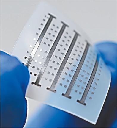
Solution‐processed metal oxide thin‐film transistors (TFTs) represent a promising technology for applications in existing but also emerging large‐area electronics. However, high process temperatures and lengthy annealing times represent two remaining technical challenges. Different approaches aiming to address these challenges have been proposed but progress remains modest. Here, the development of high electron mobility metal oxide TFTs based on photonically converted Al2O3/ZrO2 and In2O3/ZnO bilayers acting as the high‐k dielectric and electron‐transporting channel, respectively is described. Sequential solution‐phase deposition and photonic processing lead to low substrate temperature (<200 °C) while minimizing the overall process time to less than 60 s without compromising the quality of the formed layers. The bilayer Al2O3/ZrO2 dielectric exhibits low leakage current density (10−6 A cm−2 at 1 MV cm−1), high geometric capacitance (≈120 nF cm−2) and breakdown electric field of ≈1 MV cm−1. Combining Al2O3/ZrO2 with a photonically converted In2O3/ZnO heterojunction channels, results in TFTs with high electron mobility (19 cm2 V−1 s−1), low operation voltage (≤2 V), high current on/off ratio (>106), and low subthreshold swing (108 mV dec−1), that can be manufactured even onto thermally sensitive polymer substrates. The work is a significant step toward all‐photonic processed metal oxide electronics.
中文翻译:

通过快速光子处理的低压异质结金属氧化物晶体管
固溶处理的金属氧化物薄膜晶体管(TFT)代表了一种有前途的技术,可用于现有的但也正在兴起的大面积电子产品中。然而,高工艺温度和漫长的退火时间代表了剩下的两个技术挑战。已经提出了旨在解决这些挑战的不同方法,但是进展仍然不大。在这里,基于光子转换的Al 2 O 3 / ZrO 2和In 2 O 3 / ZnO双层作为高k的高电子迁移率金属氧化物TFT的发展分别描述了电介质和电子传输通道。依次进行固溶相沉积和光子处理可降低基板温度(<200°C),同时将整个处理时间降至60 s以内,而不会影响所形成层的质量。双层Al 2 O 3 / ZrO 2电介质表现出低泄漏电流密度(在1 MV cm -1时为10 -6 A cm -2),高几何电容(≈120nF cm -2)和击穿电场为≈1MV厘米-1。将Al 2 O 3 / ZrO 2与光子转换的In 2 O结合3 / ZnO异质结沟道,导致TFTs具有高电子迁移率(19 cm 2 V -1 s- 1),低工作电压(≤2V),高电流开/关比(> 10 6)和低亚阈值摆幅(108 mV dec -1),甚至可以在热敏聚合物基板上制造。这项工作是迈向全光子处理的金属氧化物电子学的重要一步。
更新日期:2020-05-08
中文翻译:
通过快速光子处理的低压异质结金属氧化物晶体管
固溶处理的金属氧化物薄膜晶体管(TFT)代表了一种有前途的技术,可用于现有的但也正在兴起的大面积电子产品中。然而,高工艺温度和漫长的退火时间代表了剩下的两个技术挑战。已经提出了旨在解决这些挑战的不同方法,但是进展仍然不大。在这里,基于光子转换的Al 2 O 3 / ZrO 2和In 2 O 3 / ZnO双层作为高k的高电子迁移率金属氧化物TFT的发展分别描述了电介质和电子传输通道。依次进行固溶相沉积和光子处理可降低基板温度(<200°C),同时将整个处理时间降至60 s以内,而不会影响所形成层的质量。双层Al 2 O 3 / ZrO 2电介质表现出低泄漏电流密度(在1 MV cm -1时为10 -6 A cm -2),高几何电容(≈120nF cm -2)和击穿电场为≈1MV厘米-1。将Al 2 O 3 / ZrO 2与光子转换的In 2 O结合3 / ZnO异质结沟道,导致TFTs具有高电子迁移率(19 cm 2 V -1 s- 1),低工作电压(≤2V),高电流开/关比(> 10 6)和低亚阈值摆幅(108 mV dec -1),甚至可以在热敏聚合物基板上制造。这项工作是迈向全光子处理的金属氧化物电子学的重要一步。


 京公网安备 11010802027423号