当前位置:
X-MOL 学术
›
ACS Cent. Sci.
›
论文详情
Our official English website, www.x-mol.net, welcomes your
feedback! (Note: you will need to create a separate account there.)
Solution-Processed, Large-Area, Two-Dimensional Crystals of Organic Semiconductors for Field-Effect Transistors and Phototransistors.
ACS Central Science ( IF 12.7 ) Pub Date : 2020-05-08 , DOI: 10.1021/acscentsci.0c00251 Cong Wang 1 , Beibei Fu 1 , Xiaotao Zhang 1 , Rongjin Li 1 , Huanli Dong 2 , Wenping Hu 1
ACS Central Science ( IF 12.7 ) Pub Date : 2020-05-08 , DOI: 10.1021/acscentsci.0c00251 Cong Wang 1 , Beibei Fu 1 , Xiaotao Zhang 1 , Rongjin Li 1 , Huanli Dong 2 , Wenping Hu 1
Affiliation
|
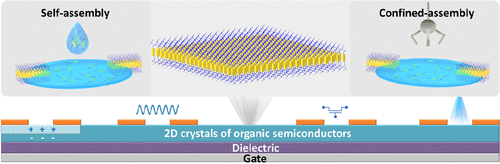
Organic electronics with π-conjugated organic semiconductors are promising candidates for the next electronics revolution. For the conductive channel, the large-area two-dimensional (2D) crystals of organic semiconductors (2DCOS) serve as useful scaffolds for modern organic electronics, benefiting not only from long-range order and low defect density nature but also from unique charge transport characteristic and photoelectrical properties. Meanwhile, the solution process with advantages of cost-effectiveness and room temperature compatibility is the foundation of high-throughput print electrical devices. Herein, we will give an insightful overview to witness the huge advances in 2DCOS over the past decade. First, the typical influencing factors and state-of-the-art assembly strategies of the solution-process for large-area 2DCOS over sub-millimeter even to wafer size are discussed accompanying rational evaluation. Then, the charge transport characteristics and contact resistance of 2DCOS-based transistors are explored. Following this, beyond single transistors, the p–n junction devices and planar integrated circuits based on 2DCOS are also emphasized. Furthermore, the burgeoning phototransistors (OPTs) based on crystals in the 2D limits are elaborated. Next, we emphasized the unique and enhanced photoelectrical properties based on a hybrid system with other 2D van der Waals solids. Finally, frontier insights and opportunities are proposed, promoting further research in this field.
中文翻译:

用于场效应晶体管和光电晶体管的有机半导体溶液处理的大面积二维晶体。
具有π共轭有机半导体的有机电子器件有望成为下一次电子革命的候选者。对于导电通道,有机半导体的大面积二维(2D)晶体(2DCOS)可作为现代有机电子的有用支架,不仅受益于长程有序和低缺陷密度性质,而且还受益于独特的电荷传输特性和光电性能。同时,具有成本效益和室温兼容性的优点的解决方法是高通量印刷电气设备的基础。在此,我们将提供有见地的概述,以见证过去十年来2DCOS的巨大进步。第一,结合合理的评估,讨论了亚毫米甚至晶片尺寸的大面积2DCOS解决方案的典型影响因素和最新组装策略。然后,探讨了基于2DCOS的晶体管的电荷传输特性和接触电阻。在此之后,除了单个晶体管以外,还强调了p–n结器件和基于2DCOS的平面集成电路。此外,还阐述了基于2D极限晶体的新兴光电晶体管(OPT)。接下来,我们强调基于与其他2D范德华固体的混合系统的独特和增强的光电性能。最后,提出了前沿的见识和机遇,促进了该领域的进一步研究。研究了基于2DCOS的晶体管的电荷传输特性和接触电阻。在此之后,除了单个晶体管以外,还强调了p–n结器件和基于2DCOS的平面集成电路。此外,还详细阐述了基于2D极限晶体的新兴光电晶体管(OPT)。接下来,我们强调基于与其他2D范德华固体的混合系统的独特和增强的光电性能。最后,提出了前沿的见识和机遇,促进了该领域的进一步研究。研究了基于2DCOS的晶体管的电荷传输特性和接触电阻。在此之后,除了单个晶体管以外,还强调了p–n结器件和基于2DCOS的平面集成电路。此外,还详细阐述了基于2D极限晶体的新兴光电晶体管(OPT)。接下来,我们强调基于与其他2D范德华固体的混合系统的独特和增强的光电性能。最后,提出了前沿的见识和机遇,促进了该领域的进一步研究。阐述了基于2D极限晶体的新兴光电晶体管(OPT)。接下来,我们强调基于与其他2D范德华固体的混合系统的独特和增强的光电性能。最后,提出了前沿的见识和机遇,促进了该领域的进一步研究。阐述了基于2D极限晶体的新兴光电晶体管(OPT)。接下来,我们强调基于与其他2D范德华固体的混合系统的独特和增强的光电性能。最后,提出了前沿的见识和机遇,促进了该领域的进一步研究。
更新日期:2020-05-08
中文翻译:
用于场效应晶体管和光电晶体管的有机半导体溶液处理的大面积二维晶体。
具有π共轭有机半导体的有机电子器件有望成为下一次电子革命的候选者。对于导电通道,有机半导体的大面积二维(2D)晶体(2DCOS)可作为现代有机电子的有用支架,不仅受益于长程有序和低缺陷密度性质,而且还受益于独特的电荷传输特性和光电性能。同时,具有成本效益和室温兼容性的优点的解决方法是高通量印刷电气设备的基础。在此,我们将提供有见地的概述,以见证过去十年来2DCOS的巨大进步。第一,结合合理的评估,讨论了亚毫米甚至晶片尺寸的大面积2DCOS解决方案的典型影响因素和最新组装策略。然后,探讨了基于2DCOS的晶体管的电荷传输特性和接触电阻。在此之后,除了单个晶体管以外,还强调了p–n结器件和基于2DCOS的平面集成电路。此外,还阐述了基于2D极限晶体的新兴光电晶体管(OPT)。接下来,我们强调基于与其他2D范德华固体的混合系统的独特和增强的光电性能。最后,提出了前沿的见识和机遇,促进了该领域的进一步研究。研究了基于2DCOS的晶体管的电荷传输特性和接触电阻。在此之后,除了单个晶体管以外,还强调了p–n结器件和基于2DCOS的平面集成电路。此外,还详细阐述了基于2D极限晶体的新兴光电晶体管(OPT)。接下来,我们强调基于与其他2D范德华固体的混合系统的独特和增强的光电性能。最后,提出了前沿的见识和机遇,促进了该领域的进一步研究。研究了基于2DCOS的晶体管的电荷传输特性和接触电阻。在此之后,除了单个晶体管以外,还强调了p–n结器件和基于2DCOS的平面集成电路。此外,还详细阐述了基于2D极限晶体的新兴光电晶体管(OPT)。接下来,我们强调基于与其他2D范德华固体的混合系统的独特和增强的光电性能。最后,提出了前沿的见识和机遇,促进了该领域的进一步研究。阐述了基于2D极限晶体的新兴光电晶体管(OPT)。接下来,我们强调基于与其他2D范德华固体的混合系统的独特和增强的光电性能。最后,提出了前沿的见识和机遇,促进了该领域的进一步研究。阐述了基于2D极限晶体的新兴光电晶体管(OPT)。接下来,我们强调基于与其他2D范德华固体的混合系统的独特和增强的光电性能。最后,提出了前沿的见识和机遇,促进了该领域的进一步研究。


 京公网安备 11010802027423号