当前位置:
X-MOL 学术
›
Phys. Status Solidi. Rapid Res. Lett.
›
论文详情
Our official English website, www.x-mol.net, welcomes your
feedback! (Note: you will need to create a separate account there.)
Conductivity Modulation of a Slit Channel in a Monolayer MoS2 Homostructure
Physica Status Solidi-Rapid Research Letters ( IF 2.5 ) Pub Date : 2020-05-12 , DOI: 10.1002/pssr.202000082 Xiangcong Kong 1 , Tao Li 1 , Yeming Xu 2, 3 , Lin Cao 2 , Minghui Lu 2 , Di Wu 2, 3 , Tai Min 1
Physica Status Solidi-Rapid Research Letters ( IF 2.5 ) Pub Date : 2020-05-12 , DOI: 10.1002/pssr.202000082 Xiangcong Kong 1 , Tao Li 1 , Yeming Xu 2, 3 , Lin Cao 2 , Minghui Lu 2 , Di Wu 2, 3 , Tai Min 1
Affiliation
|
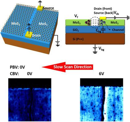
The 1D‐edge structure can potentially demonstrate higher conductivity in 2D materials because of dangling bonds and symmetry breaking. Studies use edge contact to circumvent the contact‐scaling problem in 2D field‐effect transistors (FETs) but with a rather complicated device fabrication process. Herein, a new concept is proposed directly using edges as the modulated channel, realized in a simple monolayer MoS2 homostructure. When two 1D edges lie close to each other, they form a slit, which may demonstrate distinctive electronic features. The local conductivity along naturally and artificially created slits in monolayer MoS2 is evaluated using noninvasive scanning microwave impedance microscopy with high spatial resolution. It is found that the two edges of the slits can show dramatically different conductivity due to the potential difference between the two parts separated by the slit, which can be controlled independently by the back‐gate voltage and scanning conditions. Even when the back‐gate voltage is off, the potential difference across the slit can retain, which makes it nonvolatile. This feature enables a MoS2 flake to work as a homostructure device, in which the slit can perform as an efficient channel. The findings provide an alternative perspective of using slit as a new approach for 2D electronic devices.
中文翻译:

单层MoS2同质结构中狭缝通道的电导率调制
由于悬空键和对称断裂,一维边缘结构可能在二维材料中显示出更高的电导率。研究使用边缘接触来规避2D场效应晶体管(FET)中的接触缩放问题,但器件制造过程相当复杂。在此,提出了直接使用边缘作为调制通道的新概念,该概念以简单的单层MoS 2同质结构实现。当两个1D边缘彼此靠近时,它们会形成一条狭缝,这可能显示出独特的电子功能。沿单层MoS 2中自然和人工创建的狭缝的局部电导率使用具有高空间分辨率的非侵入性扫描微波阻抗显微镜对射线进行评估。发现狭缝的两个边缘由于被狭缝分开的两个部分之间的电势差而可以显示出显着不同的导电性,这可以通过背栅电压和扫描条件独立地控制。即使关闭背栅电压,狭缝上的电势差也可以保留,这使其不易挥发。此功能使MoS 2薄片可以用作均质结构设备,其中缝隙可以用作有效通道。这些发现提供了将狭缝用作2D电子设备新方法的另一种观点。
更新日期:2020-05-12
中文翻译:
单层MoS2同质结构中狭缝通道的电导率调制
由于悬空键和对称断裂,一维边缘结构可能在二维材料中显示出更高的电导率。研究使用边缘接触来规避2D场效应晶体管(FET)中的接触缩放问题,但器件制造过程相当复杂。在此,提出了直接使用边缘作为调制通道的新概念,该概念以简单的单层MoS 2同质结构实现。当两个1D边缘彼此靠近时,它们会形成一条狭缝,这可能显示出独特的电子功能。沿单层MoS 2中自然和人工创建的狭缝的局部电导率使用具有高空间分辨率的非侵入性扫描微波阻抗显微镜对射线进行评估。发现狭缝的两个边缘由于被狭缝分开的两个部分之间的电势差而可以显示出显着不同的导电性,这可以通过背栅电压和扫描条件独立地控制。即使关闭背栅电压,狭缝上的电势差也可以保留,这使其不易挥发。此功能使MoS 2薄片可以用作均质结构设备,其中缝隙可以用作有效通道。这些发现提供了将狭缝用作2D电子设备新方法的另一种观点。


 京公网安备 11010802027423号