Materials Science and Engineering: B ( IF 3.9 ) Pub Date : 2020-05-07 , DOI: 10.1016/j.mseb.2020.114559 Hammed Ejalonibu , Gordon Sarty , Michael Bradley
|
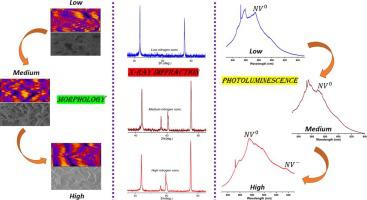
Optical centres embedded via nitrogen doping in polycrystalline diamonds (PCDs) are becoming increasingly useful for several wide-area applications including magnetic field sensing. Therefore, investigating the effect of step-wise surface nitrogen doping in PCDs deposited at low pressure is essential. In this study, the influence of a step-wise surface nitrogen doping process on PCDs has been investigated to explain the dominance of neutral charged NV (NV0) centres in PCDs deposited at low pressure in a chemical vapour deposition (CVD) chamber. The surface properties of the films were probed using Raman spectroscopy, Photoluminescence spectroscopy (PL), Scanning Electron Microscopy (SEM), Atomic Force Microscopy (AFM), X-ray Photoelectron Spectroscopy (XPS) and Grazing Incidence X-ray Diffractogram (GIXRD). The results obtained from Raman analysis and corroborated by SEM micrographs show the formation of nanocrystalline diamonds (NCDs) with a large quantity of /a-C (amorphous carbon) phases at low nitrogen flow rates on the surface of the doped PCDs. Conversely, increasing nitrogen flow rate ([N/C] > 0.0025) reduced the formation of nano-grains resulting in a decrease in the /a-C contents in the grains and grain boundaries. The increase in the [N/C] ratio and a decrease in the /a-C content at a high surface nitrogen flow rate (10 sccm) enhanced the formation of negatively charged nitrogen-vacancy (NV−) centres. Furthermore, it was shown that the occurrence of stable NV− centres in PCDs deposited at low pressure is also a function of the grain boundary line density: grain boundary line density increases at low surface nitrogen concentration thereby quenching the PL intensity of NV− centres. Samples doped with high surface nitrogen have surface roughness of less than 10 nm. The low surface roughness of highly doped films will optimize the performance of magnetometers that uses these diamond films as NV detectors. Our results give a better understanding of the formation of negatively charged NV centres in PCDs deposited at low pressure.
中文翻译:
逐步表面氮掺杂对MPECVD生长的多晶金刚石的影响
通过氮掺杂嵌入多晶金刚石(PCD)中的光学中心在包括磁场传感在内的多种广域应用中正变得越来越有用。因此,研究在低压下沉积的PCD中逐步进行表面氮掺杂的效果至关重要。在这项研究中,研究了逐步进行的表面氮掺杂工艺对PCD的影响,以解释中性带电NV(NV 0)的中心位于在化学气相沉积(CVD)室中低压沉积的PCD中。使用拉曼光谱,光致发光光谱(PL),扫描电子显微镜(SEM),原子力显微镜(AFM),X射线光电子能谱(XPS)和掠入射X射线衍射图(GIXRD)探测薄膜的表面性能。 。拉曼分析获得的结果得到SEM显微照片的证实,结果表明形成了大量纳米晶金刚石(NCD)。在掺杂的PCD的表面上以低氮气流速形成/ aC(无定形碳)相。相反,增加氮气流量([N / C]> 0.0025)减少了纳米颗粒的形成,从而降低了/ aC含量在晶粒和晶界中。[N / C]比增加,而[N / C]比减少/ AC内容在增强带负电的氮空位的(NV形成高表面氮气流速(10sccm的)- )中心。此外,结果表明,稳定NV的发生-保藏在低压中心在个人通讯装置也是晶粒边界线密度的函数:在低表面氮浓度从而淬灭NV的PL强度晶粒边界线密度的增加-中心。掺杂有高表面氮的样品的表面粗糙度小于10 nm。高掺杂薄膜的低表面粗糙度将优化磁力计的性能,磁力计将这些金刚石薄膜用作NV检测器。我们的结果更好地了解了低压沉积的PCD中带负电的NV中心的形成。


 京公网安备 11010802027423号