当前位置:
X-MOL 学术
›
Mater. Horiz.
›
论文详情
Our official English website, www.x-mol.net, welcomes your
feedback! (Note: you will need to create a separate account there.)
Direct laser-patterned MXene–perovskite image sensor arrays for visible-near infrared photodetection
Materials Horizons ( IF 12.2 ) Pub Date : 2020-05-01 , DOI: 10.1039/d0mh00537a Aobo Ren 1, 2, 3, 4 , Jihua Zou 1, 2, 3, 4 , Huagui Lai 4, 5, 6, 7, 8 , Yixuan Huang 1, 2, 3, 4 , Liming Yuan 1, 2, 3, 4 , Hao Xu 1, 2, 3, 4 , Kai Shen 9, 10, 11, 12 , Hao Wang 12, 13, 14, 15, 16 , Shunyong Wei 1, 2, 3, 4 , Yunfan Wang 4, 5, 6, 7, 8 , Xia Hao 4, 5, 6, 7, 8 , Jingquan Zhang 4, 5, 6, 7, 8 , Dewei Zhao 4, 5, 6, 7, 8 , Jiang Wu 1, 2, 3, 4 , Zhiming Wang 1, 2, 3, 4
Materials Horizons ( IF 12.2 ) Pub Date : 2020-05-01 , DOI: 10.1039/d0mh00537a Aobo Ren 1, 2, 3, 4 , Jihua Zou 1, 2, 3, 4 , Huagui Lai 4, 5, 6, 7, 8 , Yixuan Huang 1, 2, 3, 4 , Liming Yuan 1, 2, 3, 4 , Hao Xu 1, 2, 3, 4 , Kai Shen 9, 10, 11, 12 , Hao Wang 12, 13, 14, 15, 16 , Shunyong Wei 1, 2, 3, 4 , Yunfan Wang 4, 5, 6, 7, 8 , Xia Hao 4, 5, 6, 7, 8 , Jingquan Zhang 4, 5, 6, 7, 8 , Dewei Zhao 4, 5, 6, 7, 8 , Jiang Wu 1, 2, 3, 4 , Zhiming Wang 1, 2, 3, 4
Affiliation
|
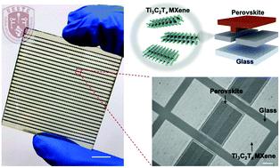
Solution-processed materials, including halide perovskites and newly discovered MXenes, are emerging as promising candidates for next-generation optoelectronic devices. Here, large-scale image sensor arrays (1250 pixels) based on a MXene/perovskite/MXene structure are demonstrated by utilizing top-down techniques, i.e. spin-coating and laser-scribing. The work allows processing perovskite and MXene materials into sub-millimeter photodetector arrays on a large scale with potential for further down-scaling of the device dimensions. The favorable energy level alignment and resonance enhancement of such materials enable efficient charge transfer and detection up to the near infrared region. A high responsivity of 84.77 A W−1, a high specific detectivity of 3.22 × 10¹² Jones, and a large linear dynamic range (LDR) up to 82 dB in a broadband wavelength range from visible to near-infrared are achieved. In addition, the device shows an excellent image-capture capability under near infrared illumination. Given the tunability and compatibility with complementary metal–oxide–semiconductors (CMOS), the method potentially promotes the development of low-cost, high-performance, and large format photodetector arrays.
中文翻译:

直接激光图案化的MXene-钙钛矿图像传感器阵列,用于可见-近红外光电检测
溶液加工的材料,包括卤化钙钛矿和新发现的MXene,正在成为下一代光电子器件的有前途的候选材料。在此,通过利用自上而下的技术(即旋涂和激光划刻)展示了基于MXene /钙钛矿/ MXene结构的大规模图像传感器阵列(1250像素)。这项工作可以将钙钛矿和MXene材料大规模加工成亚毫米级光电探测器阵列,并有可能进一步缩小器件尺寸。这种材料的有利的能级对准和共振增强使得能够进行有效的电荷转移和检测直至近红外区域。高响应度为84.77 AW -1,高比检测度为3.22×10 12琼斯(Jones),以及从可见光到近红外的宽带波长范围内达到82 dB的大线性动态范围(LDR)。此外,该器件在近红外照明下显示出出色的图像捕获能力。考虑到与互补金属氧化物半导体(CMOS)的可调谐性和兼容性,该方法潜在地促进了低成本,高性能和大幅面光电探测器阵列的发展。
更新日期:2020-07-06
中文翻译:
直接激光图案化的MXene-钙钛矿图像传感器阵列,用于可见-近红外光电检测
溶液加工的材料,包括卤化钙钛矿和新发现的MXene,正在成为下一代光电子器件的有前途的候选材料。在此,通过利用自上而下的技术(即旋涂和激光划刻)展示了基于MXene /钙钛矿/ MXene结构的大规模图像传感器阵列(1250像素)。这项工作可以将钙钛矿和MXene材料大规模加工成亚毫米级光电探测器阵列,并有可能进一步缩小器件尺寸。这种材料的有利的能级对准和共振增强使得能够进行有效的电荷转移和检测直至近红外区域。高响应度为84.77 AW -1,高比检测度为3.22×10 12琼斯(Jones),以及从可见光到近红外的宽带波长范围内达到82 dB的大线性动态范围(LDR)。此外,该器件在近红外照明下显示出出色的图像捕获能力。考虑到与互补金属氧化物半导体(CMOS)的可调谐性和兼容性,该方法潜在地促进了低成本,高性能和大幅面光电探测器阵列的发展。


 京公网安备 11010802027423号