当前位置:
X-MOL 学术
›
Int. J. Circ. Theory Appl.
›
论文详情
Our official English website, www.x-mol.net, welcomes your
feedback! (Note: you will need to create a separate account there.)
A charge‐sharing analog‐to‐digital converter with embedded downconversion using a variable reference voltage
International Journal of Circuit Theory and Applications ( IF 1.8 ) Pub Date : 2020-04-15 , DOI: 10.1002/cta.2793 Nuno Pereira 1, 2 , João Goes 1, 2
International Journal of Circuit Theory and Applications ( IF 1.8 ) Pub Date : 2020-04-15 , DOI: 10.1002/cta.2793 Nuno Pereira 1, 2 , João Goes 1, 2
Affiliation
|
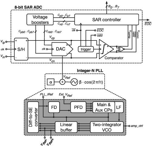
In the field of radio receivers, downconversion methods usually rely on one (or more) explicit mixing stage(s) before the analog‐to‐digital converter (ADC). These stages not only contribute to the overall power consumption but also have an impact on area and can compromise the converter's performance in terms of noise and linearity. As an alternative, we propose a receiver architecture that considers the ADC as both a quantizer and a downconverter block. This is achieved through the use of a variable reference signal (in this case, a voltage), as opposed to classic time‐invariant reference signals. When embedded into a charge‐sharing (CS) successive approximation register (SAR) ADC, this varying reference voltage is “saved” in the digital‐to‐analog converter (DAC) capacitor bank during the sampling phase, preventing any conversion errors. Furthermore, a phase‐locked loop (PLL) is used in order to provide an on‐chip solution for the generation of this variable reference voltage, which also removes the need for dedicated bandgap circuits and reference buffers. Post‐layout simulations of an 8‐bit 50 MS/s CS‐SAR ADC show that the proposed “embedded mixing” technique is able to downconvert a high‐frequency signal while also increasing the effective resolution by around 0.5 bits, when compared with a standard DC reference voltage.
中文翻译:

具有可变参考电压且具有嵌入式下变频的电荷共享模数转换器
在无线电接收机领域,下变频方法通常依赖于模数转换器(ADC)之前的一个(或多个)显式混合级。这些级不仅会影响总功耗,还会影响面积,并且会在噪声和线性度方面影响转换器的性能。作为替代方案,我们提出了一种接收器架构,该架构将ADC视为量化器和下变频器模块。与经典的时不变参考信号相反,这是通过使用可变参考信号(在这种情况下为电压)来实现的。当嵌入到电荷共享(CS)逐次逼近寄存器(SAR)ADC中时,该变化的参考电压在采样阶段被“保存”在数模转换器(DAC)电容器组中,从而防止了任何转换错误。此外,使用锁相环(PLL)来提供用于生成此可变参考电压的片上解决方案,这也消除了对专用带隙电路和参考缓冲器的需求。与8位50 MS / s CS-SAR ADC的布局后仿真显示,所建议的“嵌入式混频”技术能够对高频信号进行降频转换,同时与使用A / D转换器相比,还能将有效分辨率提高约0.5位。标准直流参考电压。
更新日期:2020-04-15
中文翻译:
具有可变参考电压且具有嵌入式下变频的电荷共享模数转换器
在无线电接收机领域,下变频方法通常依赖于模数转换器(ADC)之前的一个(或多个)显式混合级。这些级不仅会影响总功耗,还会影响面积,并且会在噪声和线性度方面影响转换器的性能。作为替代方案,我们提出了一种接收器架构,该架构将ADC视为量化器和下变频器模块。与经典的时不变参考信号相反,这是通过使用可变参考信号(在这种情况下为电压)来实现的。当嵌入到电荷共享(CS)逐次逼近寄存器(SAR)ADC中时,该变化的参考电压在采样阶段被“保存”在数模转换器(DAC)电容器组中,从而防止了任何转换错误。此外,使用锁相环(PLL)来提供用于生成此可变参考电压的片上解决方案,这也消除了对专用带隙电路和参考缓冲器的需求。与8位50 MS / s CS-SAR ADC的布局后仿真显示,所建议的“嵌入式混频”技术能够对高频信号进行降频转换,同时与使用A / D转换器相比,还能将有效分辨率提高约0.5位。标准直流参考电压。


 京公网安备 11010802027423号