当前位置:
X-MOL 学术
›
Phys. Status Solidi A
›
论文详情
Our official English website, www.x-mol.net, welcomes your
feedback! (Note: you will need to create a separate account there.)
Comparison of Strain Characteristics and Contact Resistances of Heavily Phosphorus‐Doped Si Formed by Phosphorus Implantation and In Situ Phosphorus‐Doped Si Epitaxial Growth
Physica Status Solidi (A) - Applications and Materials Science Pub Date : 2020-03-18 , DOI: 10.1002/pssa.201900989 Eunjung Ko 1, 2 , Juhee Lee 1, 2 , Hyunsu Shin 2 , Seran Park 2 , Daehong Ko 2
Physica Status Solidi (A) - Applications and Materials Science Pub Date : 2020-03-18 , DOI: 10.1002/pssa.201900989 Eunjung Ko 1, 2 , Juhee Lee 1, 2 , Hyunsu Shin 2 , Seran Park 2 , Daehong Ko 2
Affiliation
|
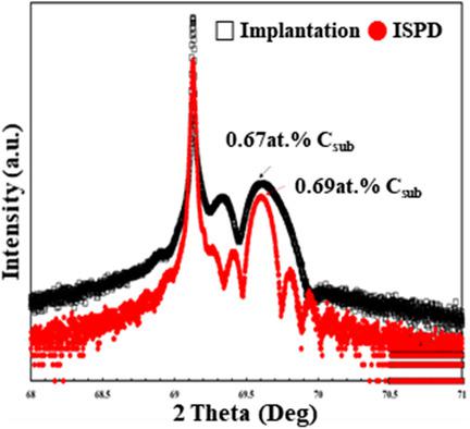
As transistor sizes reduce, the effect of contact resistivity on power consumption increases. To reduce contact resistivity, heavily phosphorus‐doped Si grown via in situ phosphorus‐doped (ISPD) Si epitaxial growth is studied actively. Laser spike annealing to the heavily phosphorus implanted (IMP) layers is demonstrated to replace ISPD Si epitaxial growth process and phosphorus profiles and strain characteristics are evaluated. Regardless of the doping method, the phosphorus concentrations of both samples and their tensile strains are equivalent. After laser annealing, the metal‐silicidation is conducted to measure contact resistivity. The Ni‐silicide formed on IMP sample has 3D clusters inducing greater morphological degradation than ISPD samples. The contact resistivity of IMP sample measured using the circular transmission line model (CTLM) (1.2–8.3 × 10⁻⁸ Ω cm2) is similar to that of the ISPD sample (1.1–5.5 × 10⁻⁸ Ω cm2) after Ni‐silicidation of the ISPD layer. This study performs strain engineering by achieving low contact resistance at lower cost while applying strain using the IMP process rather than the epitaxial process.
中文翻译:

磷注入和原位掺磷硅外延生长形成的重掺磷硅的应变特性和接触电阻的比较
随着晶体管尺寸的减小,接触电阻率对功耗的影响增加。为降低接触电阻率,积极研究了通过原位掺磷(ISPD)Si外延生长生长的重掺磷Si。证明了对重注入磷(IMP)层的激光尖峰退火可以替代ISPD Si外延生长工艺,并评估了磷的分布和应变特性。无论采用哪种掺杂方法,两个样品的磷浓度及其拉伸应变均相等。激光退火后,进行金属硅化处理以测量接触电阻率。与ISPD样品相比,在IMP样品上形成的镍硅化物具有3D团簇,可引起更大的形态学降解。使用圆形传输线模型(CTLM)测量的IMP样品的接触电阻率(1。-8 Ω厘米2)是类似于ISPD样品(1.1-5.5×10 -8 Ω厘米2的ISPD层的镍硅化之后)。这项研究通过以较低的成本实现低接触电阻来执行应变工程,同时使用IMP工艺而非外延工艺施加应变。
更新日期:2020-03-18
中文翻译:
磷注入和原位掺磷硅外延生长形成的重掺磷硅的应变特性和接触电阻的比较
随着晶体管尺寸的减小,接触电阻率对功耗的影响增加。为降低接触电阻率,积极研究了通过原位掺磷(ISPD)Si外延生长生长的重掺磷Si。证明了对重注入磷(IMP)层的激光尖峰退火可以替代ISPD Si外延生长工艺,并评估了磷的分布和应变特性。无论采用哪种掺杂方法,两个样品的磷浓度及其拉伸应变均相等。激光退火后,进行金属硅化处理以测量接触电阻率。与ISPD样品相比,在IMP样品上形成的镍硅化物具有3D团簇,可引起更大的形态学降解。使用圆形传输线模型(CTLM)测量的IMP样品的接触电阻率(1。-8 Ω厘米2)是类似于ISPD样品(1.1-5.5×10 -8 Ω厘米2的ISPD层的镍硅化之后)。这项研究通过以较低的成本实现低接触电阻来执行应变工程,同时使用IMP工艺而非外延工艺施加应变。


 京公网安备 11010802027423号