当前位置:
X-MOL 学术
›
J. Soc. Inf. Disp.
›
论文详情
Our official English website, www.x-mol.net, welcomes your feedback! (Note: you will need to create a separate account there.)
Two‐stage degradation in n‐channel LTPS‐TFTs under negative and positive bias stresses
Journal of the Society for Information Display ( IF 2.3 ) Pub Date : 2020-01-26 , DOI: 10.1002/jsid.873 Jian Guo 1 , Zhinong Yu 1 , Wei Yan 1 , Dawei Shi 2 , Jianshe Xue 2 , Wei Xue 1
Journal of the Society for Information Display ( IF 2.3 ) Pub Date : 2020-01-26 , DOI: 10.1002/jsid.873 Jian Guo 1 , Zhinong Yu 1 , Wei Yan 1 , Dawei Shi 2 , Jianshe Xue 2 , Wei Xue 1
Affiliation
|
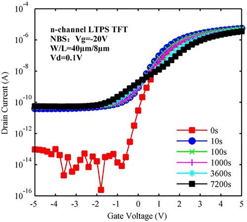
Device degradation behaviors of n‐channel low‐temperature polycrystalline silicon thin film transistors under negative bias stress and positive bias stress were investigated. It was found that the threshold‐voltage has a two‐stage degradation, shifting to different direction with time. The mobility and the subthreshold swing SS both show a dependence on the stress time. It was determined that the interface trap states, the grain boundary trap states, and electron trapping together dominate the time‐dependent degradation behaviors. The trap is caused by the rupture of Si─H and Si─O bonds. A comprehensive model is proposed to explain the time‐dependent degradation behaviors clearly. In addition, after removing the stress, the recovery behaviors of threshold voltage Vth can be observed, which provide the evidence supporting the degradation model proposed.
中文翻译:

负偏压和正偏压下n沟道LTPS-TFT的两阶段退化
研究了n沟道低温多晶硅薄膜晶体管在负偏压和正偏压下的器件退化行为。发现阈值电压具有两级衰减,随时间变化到不同的方向。迁移率和亚阈值摆动SS都显示出对应力时间的依赖性。可以确定,界面陷阱态,晶界陷阱态和电子陷阱共同主导了随时间变化的降解行为。陷阱是由Si-H和Si-O键的断裂引起的。提出了一个综合模型来清楚地解释随时间变化的退化行为。另外,去除应力后,阈值电压V th的恢复行为 可以观察到,这提供了支持所提出的退化模型的证据。
更新日期:2020-01-26
中文翻译:
负偏压和正偏压下n沟道LTPS-TFT的两阶段退化
研究了n沟道低温多晶硅薄膜晶体管在负偏压和正偏压下的器件退化行为。发现阈值电压具有两级衰减,随时间变化到不同的方向。迁移率和亚阈值摆动SS都显示出对应力时间的依赖性。可以确定,界面陷阱态,晶界陷阱态和电子陷阱共同主导了随时间变化的降解行为。陷阱是由Si-H和Si-O键的断裂引起的。提出了一个综合模型来清楚地解释随时间变化的退化行为。另外,去除应力后,阈值电压V th的恢复行为 可以观察到,这提供了支持所提出的退化模型的证据。


 京公网安备 11010802027423号