当前位置:
X-MOL 学术
›
Mater. Today Phys.
›
论文详情
Our official English website, www.x-mol.net, welcomes your
feedback! (Note: you will need to create a separate account there.)
Thermoelectric Properties of Holey Silicon at Elevated Temperatures
Materials Today Physics ( IF 10.0 ) Pub Date : 2020-08-01 , DOI: 10.1016/j.mtphys.2020.100224 N. Liu , T. Zhu , M.G. Rosul , J. Peters , J.E. Bowers , M. Zebarjadi
Materials Today Physics ( IF 10.0 ) Pub Date : 2020-08-01 , DOI: 10.1016/j.mtphys.2020.100224 N. Liu , T. Zhu , M.G. Rosul , J. Peters , J.E. Bowers , M. Zebarjadi
|
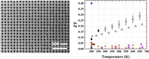
Abstract Compatibility to the semiconductor industry makes silicon thin-film devices attractive for thermoelectric applications. Silicon has a competitive thermoelectric power factor but a large thermal conductivity, which results in an overall small thermoelectric figure of merit, ZT. By patterning arrays of nano-sized holes with spacing less than the average phonon mean free path into the Si thin films, their thermal conductivity can be greatly suppressed, whereas their electronic properties are less affected. We fabricated and measured the electronic and thermal transport properties of such holey Si devices from 300 K to 650 K. Heat diffusion imaging, a hybrid approach that combines thermoreflectance imaging and the heat spreader method was used for the in-plane thermal conductivity measurement and gives a value of 6.00 ± 1.83 W/mK at room temperature. The power factor times temperature is about 0.52 ± 0.04 W/mK at 300 K and 1.10 ± 0.09 W/mK at 650 K. Therefore, ZT of the holey Si device is approximately 0.09 at room temperature and is at least 0.29 at 650 K. Further improvement is possible by optimizing the feature sizes and using surface doping.
中文翻译:

高温下多孔硅的热电特性
摘要 与半导体行业的兼容性使硅薄膜器件对热电应用具有吸引力。硅具有具有竞争力的热电功率因数,但具有较大的热导率,这导致整体热电品质因数 ZT 较小。通过将间距小于平均声子平均自由程的纳米孔阵列图案化到 Si 薄膜中,它们的热导率可以被大大抑制,而它们的电子特性受到的影响较小。我们制造并测量了这种多孔 Si 器件从 300 K 到 650 K 的电子和热传输特性。 热扩散成像是一种结合热反射成像和散热器方法的混合方法,用于面内热导率测量,并给出值为 6.00 ± 1。在室温下为 83 W/mK。功率因数乘以温度在 300 K 时约为 0.52 ± 0.04 W/mK,在 650 K 时约为 1.10 ± 0.09 W/mK。因此,多孔硅器件的 ZT 在室温下约为 0.09,在 650 K 时至少为 0.29。通过优化特征尺寸和使用表面掺杂可以进一步改进。
更新日期:2020-08-01
中文翻译:
高温下多孔硅的热电特性
摘要 与半导体行业的兼容性使硅薄膜器件对热电应用具有吸引力。硅具有具有竞争力的热电功率因数,但具有较大的热导率,这导致整体热电品质因数 ZT 较小。通过将间距小于平均声子平均自由程的纳米孔阵列图案化到 Si 薄膜中,它们的热导率可以被大大抑制,而它们的电子特性受到的影响较小。我们制造并测量了这种多孔 Si 器件从 300 K 到 650 K 的电子和热传输特性。 热扩散成像是一种结合热反射成像和散热器方法的混合方法,用于面内热导率测量,并给出值为 6.00 ± 1。在室温下为 83 W/mK。功率因数乘以温度在 300 K 时约为 0.52 ± 0.04 W/mK,在 650 K 时约为 1.10 ± 0.09 W/mK。因此,多孔硅器件的 ZT 在室温下约为 0.09,在 650 K 时至少为 0.29。通过优化特征尺寸和使用表面掺杂可以进一步改进。


 京公网安备 11010802027423号