Materials Today Advances ( IF 8.1 ) Pub Date : 2020-04-28 , DOI: 10.1016/j.mtadv.2020.100067 M.E.P. Tweedie , C.S. Lau , L. Hou , X. Wang , Y. Sheng , J.H. Warner
|
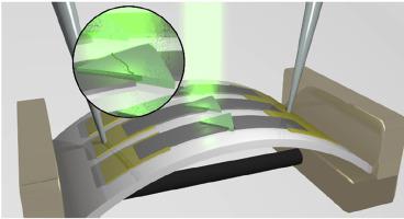
Herein, we detail developments in the scalable fabrication of all-two-dimensional (2D) flexible and transparent photodetectors. These devices were fabricated from chemical vapour deposition derived graphene and tungsten disulphide on poly(ethylene naphthalate) (PEN), a material commonly used as a substrate in flexible electronics. Alternative patterning approaches that are necessitated by the more thermally and chemically sensitive polymer substrates are explored, resulting in several modifications to conventional, silicon-substrate device fabrication approaches. In particular, the relatively new lift-off patterning approach for 2D materials is applied as an alternative to plasma etching due to the deleterious effect of plasma on the PEN substrates. This enabled the observation of a strain-modulated enhancement of photocurrent of up to one order of magnitude, demonstrating the utility of strain engineering to the field of 2D devices—provided it can be controllably applied. Further application of strain led in all cases to permanent failure and loss of photoconductivity, the details of which are explored using scanning electron microscopy. These results provide important details relevant to the fabrication of large-scale arrays of flexible and transparent 2D devices on polymer substrates.
中文翻译:
柔性基板上的透明超薄全二维横向Gr:WS 2:Gr光电探测器阵列及其应变诱发失效机理
本文中,我们详细介绍了可扩展制造的全二维(2D)柔性和透明光电探测器的发展。这些器件由化学气相沉积衍生的石墨烯和二硫化钨在聚萘二甲酸乙二醇酯(PEN)上制造而成,而聚萘二甲酸乙二醇酯通常用作柔性电子设备的基板。探索了对热和化学敏感性更高的聚合物衬底所必需的替代构图方法,从而对传统的硅衬底器件制造方法进行了多种修改。特别地,由于等离子体在PEN衬底上的有害影响,因此将相对新的用于2D材料的剥离图案化方法用作等离子体蚀刻的替代方法。这使得观察到的光电流应变调制增强高达一个数量级,从而证明了应变工程在2D设备领域的实用性—只要它可以可控制地应用。在所有情况下,进一步施加应变都会导致永久性破坏和光电导性损失,可使用扫描电子显微镜探讨其细节。这些结果提供了与在聚合物基底上大规模制造柔性和透明2D器件阵列有关的重要细节。


 京公网安备 11010802027423号