当前位置:
X-MOL 学术
›
Laser Photonics Rev.
›
论文详情
Our official English website, www.x-mol.net, welcomes your
feedback! (Note: you will need to create a separate account there.)
Single‐Layer Aberration‐Compensated Flat Lens for Robust Wide‐Angle Imaging
Laser & Photonics Reviews ( IF 9.8 ) Pub Date : 2020-04-27 , DOI: 10.1002/lpor.202000017 Chenglong Hao 1 , Shecheng Gao 2 , Qifeng Ruan 3, 4 , Yuanhua Feng 2 , Ying Li 3 , Joel K.W. Yang 4 , Zhaohui Li 5 , Cheng‐Wei Qiu 1
Laser & Photonics Reviews ( IF 9.8 ) Pub Date : 2020-04-27 , DOI: 10.1002/lpor.202000017 Chenglong Hao 1 , Shecheng Gao 2 , Qifeng Ruan 3, 4 , Yuanhua Feng 2 , Ying Li 3 , Joel K.W. Yang 4 , Zhaohui Li 5 , Cheng‐Wei Qiu 1
Affiliation
|
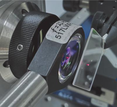
Metasurfaces are planarized and miniaturized versions of conventional optical elements. Subwavelength‐thick single‐layer metalenses have diffraction limited resolution for on‐axis imaging but relatively low resolution for off‐axis imaging due to off‐axial aberrations. The aberrations of planar single‐layer metalenses have been corrected by patterning two metasurfaces on both sides of a substrate to form metalens doublets with a thickness of hundreds of micrometers to millimeters. The multilevel diffractive lenses are demonstrated to achieve wide angle imaging with a thickness of several micrometers, however, the off‐axial aberrations are not compensated. Here, an epsilon‐greedy algorithm‐based scheme for achieving a planar wavelength‐thick single‐layer aberration‐compensated (SLAC) flat lens consisting of dielectric nanoring structures fabricated by 3D printing are proposed. The scheme is experimentally validated via a SLAC flat lens. This SLAC flat lens has a thickness of 1 µm, a numerical aperture of 0.45, a focal length of 1 mm, a full field of view (FOV) of 32° that enables aberration‐compensated imaging along the focal plane and monochromatic microscopic imaging with resolution better than 2.2 µm at a wavelength of 633 nm. This scheme can lead to ultrathin wide‐FOV flat lens designs as well as low‐cost mass production, which has various applications in miniscopes, mobile camera modules, and machine vision.
中文翻译:

单层像差补偿平面透镜,可实现强大的广角成像
超表面是常规光学元件的平面化和小型化版本。亚波长厚的单层金属感测器对于轴上成像具有衍射极限分辨率,但是由于离轴像差,离轴成像的分辨率相对较低。平面单层金属透镜的像差已通过在基板两侧上的两个超颖表面进行构图以形成厚度为数百微米至毫米的金属双合体而得到校正。多层衍射透镜可以实现几微米厚的广角成像,但是离轴像差没有得到补偿。这里,提出了一种基于epsilon-greedy算法的方案,该方案可实现由3D打印制成的电介质纳米环结构组成的平面波长厚的单层像差补偿(SLAC)平面透镜。该方案已通过SLAC平板透镜进行了实验验证。这款SLAC平面透镜的厚度为1 µm,数值孔径为0.45,焦距为1 mm,全视场(FOV)为32°,可沿焦平面进行像差补偿成像,并可以进行单色显微镜成像。在633 nm的波长下,分辨率优于2.2 µm。这种方案可以导致超薄广角FPV平面透镜设计以及低成本的批量生产,在微型显微镜,移动相机模块和机器视觉中具有多种应用。这款SLAC平面透镜的厚度为1 µm,数值孔径为0.45,焦距为1 mm,全视场(FOV)为32°,可沿焦平面进行像差补偿成像,并可以进行单色显微镜成像。在633 nm的波长下,分辨率优于2.2 µm。该方案可导致超薄广角FPV平面透镜设计以及低成本的批量生产,在微型显微镜,移动相机模块和机器视觉中具有多种应用。这款SLAC平面透镜的厚度为1 µm,数值孔径为0.45,焦距为1 mm,全视场(FOV)为32°,可沿焦平面进行像差补偿成像,并可以进行单色显微镜成像。在633 nm的波长下,分辨率优于2.2 µm。这种方案可以导致超薄广角FPV平面透镜设计以及低成本的批量生产,在微型显微镜,移动相机模块和机器视觉中具有多种应用。
更新日期:2020-04-27
中文翻译:
单层像差补偿平面透镜,可实现强大的广角成像
超表面是常规光学元件的平面化和小型化版本。亚波长厚的单层金属感测器对于轴上成像具有衍射极限分辨率,但是由于离轴像差,离轴成像的分辨率相对较低。平面单层金属透镜的像差已通过在基板两侧上的两个超颖表面进行构图以形成厚度为数百微米至毫米的金属双合体而得到校正。多层衍射透镜可以实现几微米厚的广角成像,但是离轴像差没有得到补偿。这里,提出了一种基于epsilon-greedy算法的方案,该方案可实现由3D打印制成的电介质纳米环结构组成的平面波长厚的单层像差补偿(SLAC)平面透镜。该方案已通过SLAC平板透镜进行了实验验证。这款SLAC平面透镜的厚度为1 µm,数值孔径为0.45,焦距为1 mm,全视场(FOV)为32°,可沿焦平面进行像差补偿成像,并可以进行单色显微镜成像。在633 nm的波长下,分辨率优于2.2 µm。这种方案可以导致超薄广角FPV平面透镜设计以及低成本的批量生产,在微型显微镜,移动相机模块和机器视觉中具有多种应用。这款SLAC平面透镜的厚度为1 µm,数值孔径为0.45,焦距为1 mm,全视场(FOV)为32°,可沿焦平面进行像差补偿成像,并可以进行单色显微镜成像。在633 nm的波长下,分辨率优于2.2 µm。该方案可导致超薄广角FPV平面透镜设计以及低成本的批量生产,在微型显微镜,移动相机模块和机器视觉中具有多种应用。这款SLAC平面透镜的厚度为1 µm,数值孔径为0.45,焦距为1 mm,全视场(FOV)为32°,可沿焦平面进行像差补偿成像,并可以进行单色显微镜成像。在633 nm的波长下,分辨率优于2.2 µm。这种方案可以导致超薄广角FPV平面透镜设计以及低成本的批量生产,在微型显微镜,移动相机模块和机器视觉中具有多种应用。


 京公网安备 11010802027423号