当前位置:
X-MOL 学术
›
Curr. Appl. Phys.
›
论文详情
Our official English website, www.x-mol.net, welcomes your
feedback! (Note: you will need to create a separate account there.)
Characteristics of a type-II n-MoS2/p-Ge van der Waals heterojunction
Current Applied Physics ( IF 2.4 ) Pub Date : 2020-06-01 , DOI: 10.1016/j.cap.2020.03.018 Donghwan Kim , ChaeHo Shin , Joo Hyung Park , Jonghoo Park , TaeWan Kim
Current Applied Physics ( IF 2.4 ) Pub Date : 2020-06-01 , DOI: 10.1016/j.cap.2020.03.018 Donghwan Kim , ChaeHo Shin , Joo Hyung Park , Jonghoo Park , TaeWan Kim
|
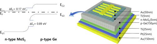
Abstract A few-atomic-layer molybdenum disulfide (MoS2) film on Si/SiO2 substrates grown by metal-organic chemical vapor deposition was investigated. The few-atomic-layer MoS2 film was subsequently transferred onto a (100) p-Ge substrate to build a van der Waals n-p heterojunction. The as-grown few-atomic-layer MoS2 film and the MoS2/Ge heterostructure were characterized atomic force microscopy, spectroscopic ellipsometry, high-resolution scanning transmission electron microscopy, Raman spectroscopy analyses, photoluminescence (PL) measurements at room temperature (RT, 300 K), and type-II band alignment of the heterostructure determined by ultraviolet photoelectron spectroscopy. The RT-PL measurements showed dominant peaks at 1.96 and 1.8 eV for the as-grown MoS2 and red-shifted PL peaks for that transferred onto Ge. We examined the electrical characteristics of the few-atomic-layer MoS2 by forming a type-II band alignment van der Waals heterojunction with a highly doped p-Ge. The heterojunction solar cell exhibited an open-circuit voltage of 0.15 V and a short-circuit current density of 45.26 μA/cm2. The external quantum efficiency measurements showed a spectral response up to approximately 500 nm owing to the absorption by the few-atomic-layer MoS2 film.
中文翻译:

II 型 n-MoS2/p-Ge 范德华异质结的特性
摘要 研究了通过金属有机化学气相沉积在 Si/SiO2 衬底上生长的少原子层二硫化钼 (MoS2) 薄膜。随后将少原子层的 MoS2 膜转移到 (100) p-Ge 衬底上以构建范德华 np 异质结。通过原子力显微镜、光谱椭偏仪、高分辨率扫描透射电子显微镜、拉曼光谱分析、室温下的光致发光 (PL) 测量 (RT, 300 K),以及由紫外光电子能谱确定的异质结构的 II 型能带排列。RT-PL 测量显示,生长的 MoS2 的主峰位于 1.96 eV 和 1.8 eV,而转移到 Ge 上的 PL 峰发生红移。我们通过形成具有高度掺杂的 p-Ge 的 II 型能带对准范德华异质结来检查少原子层 MoS2 的电气特性。异质结太阳能电池的开路电压为0.15 V,短路电流密度为45.26 μA/cm2。由于少原子层 MoS2 薄膜的吸收,外部量子效率测量显示出高达约 500 nm 的光谱响应。
更新日期:2020-06-01
中文翻译:
II 型 n-MoS2/p-Ge 范德华异质结的特性
摘要 研究了通过金属有机化学气相沉积在 Si/SiO2 衬底上生长的少原子层二硫化钼 (MoS2) 薄膜。随后将少原子层的 MoS2 膜转移到 (100) p-Ge 衬底上以构建范德华 np 异质结。通过原子力显微镜、光谱椭偏仪、高分辨率扫描透射电子显微镜、拉曼光谱分析、室温下的光致发光 (PL) 测量 (RT, 300 K),以及由紫外光电子能谱确定的异质结构的 II 型能带排列。RT-PL 测量显示,生长的 MoS2 的主峰位于 1.96 eV 和 1.8 eV,而转移到 Ge 上的 PL 峰发生红移。我们通过形成具有高度掺杂的 p-Ge 的 II 型能带对准范德华异质结来检查少原子层 MoS2 的电气特性。异质结太阳能电池的开路电压为0.15 V,短路电流密度为45.26 μA/cm2。由于少原子层 MoS2 薄膜的吸收,外部量子效率测量显示出高达约 500 nm 的光谱响应。


 京公网安备 11010802027423号