Nature Electronics ( IF 34.3 ) Pub Date : 2020-04-06 , DOI: 10.1038/s41928-020-0391-2 Ryan Hensleigh , Huachen Cui , Zhenpeng Xu , Jeffrey Massman , Desheng Yao , John Berrigan , Xiaoyu Zheng
|
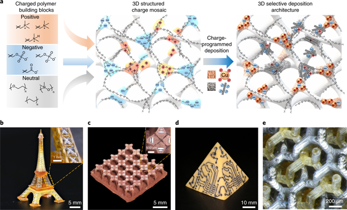
Three-dimensional (3D) printing can create complex geometries that could be of use in the development of electronics. However, the approach is mainly limited to non-functional structural materials, and the 3D printing of electronic devices typically requires multiple process stages of embedding, spraying and writing. Here, we report a 3D printing approach that can volumetrically deposit multiple functional materials within arbitrary 3D layouts to create electronic devices in a single step. Our approach prints 3D structures with a programmable mosaic of distinct surface charge regions, creating a platform to deposit functional materials into complex architectures based on localized electrostatic attraction. The technique allows selective volumetric depositions of single metals and also diverse active material combinations, including ceramic, semiconducting, magnetic and colloidal materials, into site-specific 3D topologies. To illustrate the capabilities of our approach, we use it to fabricate devices with 3D electronic interfaces that can be used for tactile sensing, internal wave mapping and shape self-sensing.
中文翻译:
用于多种材料电子设备的带电荷程序的三维打印
三维(3D)打印可以创建复杂的几何形状,这些几何形状可用于电子产品的开发。然而,该方法主要限于非功能性结构材料,并且电子设备的3D打印通常需要嵌入,喷涂和书写的多个处理阶段。在这里,我们报告了一种3D打印方法,该方法可以在任意3D布局中按体积沉积多种功能材料,从而在一个步骤中创建电子设备。我们的方法可打印带有不同表面电荷区域的可编程镶嵌图的3D结构,从而创建一个基于局部静电吸引将功能材料沉积到复杂结构中的平台。该技术可以选择性地对单个金属进行体积沉积,还可以实现多种活性材料组合,包括陶瓷,将半导体,磁性和胶体材料转换为特定于位置的3D拓扑。为了说明我们的方法的功能,我们使用它来制造具有3D电子接口的设备,这些设备可用于触觉感应,内部波形映射和形状自感应。


 京公网安备 11010802027423号