当前位置:
X-MOL 学术
›
Adv. Mater. Technol.
›
论文详情
Our official English website, www.x-mol.net, welcomes your
feedback! (Note: you will need to create a separate account there.)
Nanopaper‐Based Organic Inkjet‐Printed Diodes
Advanced Materials Technologies ( IF 6.4 ) Pub Date : 2020-04-02 , DOI: 10.1002/admt.201900773 Silvia Conti 1, 2 , Carme Martínez‐Domingo 2 , Makara Lay 3 , Lluís Terés 2 , Fabiola Vilaseca 4, 5 , Eloi Ramon 2
Advanced Materials Technologies ( IF 6.4 ) Pub Date : 2020-04-02 , DOI: 10.1002/admt.201900773 Silvia Conti 1, 2 , Carme Martínez‐Domingo 2 , Makara Lay 3 , Lluís Terés 2 , Fabiola Vilaseca 4, 5 , Eloi Ramon 2
Affiliation
|
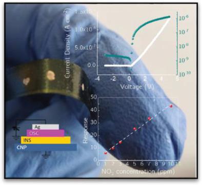
The rise of internet of things (IoTs) applications has led to the development of a new generation of light‐weight, flexible, and cost‐effective electronics. These devices and sensors have to be simultaneously easily replaceable and disposable while being environmentally sustainable. Thus, the introduction of new functionalized materials with mechanical flexibility that can be processed using large‐area and facile fabrication methods (as, for example, printing technologies) has become a matter of great interest in the scientific community. In this context, cellulose nanofibers (CNFs) are renewable, affordable, robust, and nontoxic materials that are rapidly emerging as components for eco‐friendly electronics. Their combination with conductive polymers (CPs) to obtain conductive nanopapers (CNPs) allows moving their functionality from just substrates to active components of the device. In this work, a route for the inkjet‐printing of organic diodes is outlined. The proposed strategy is based on the use of CNPs as both substrates and bottom electrodes onto which insulator and organic semiconducting layers are deposited to fabricate novel diode structures. Remarkable rectification ratios of up to 1.2 × 10³ at |3 V| and a current density up to 5.1 µA cm−2 are achieved. As a proof‐of‐concept of the potentiality of the approach for versatile, low‐temperature, and disposable sensing applications, an NO2 gas sensor is presented.
中文翻译:

基于纳米纸的有机喷墨印刷二极管
物联网(IoT)应用程序的兴起导致了新一代轻便,灵活且经济高效的电子产品的开发。这些设备和传感器必须同时易于更换和一次性使用,同时要在环境上可持续。因此,引入具有机械柔韧性的新型功能化材料,可以使用大面积且简便的制造方法(例如印刷技术)进行处理,已成为科学界的关注点。在这种情况下,纤维素纳米纤维(CNF)是可再生,价格适中,坚固且无毒的材料,并迅速成为环保电子产品的组成部分。它们与导电聚合物(CP)的组合以获得导电纳米纸(CNP),可以将其功能从仅基板转移到设备的有源组件。在这项工作中,概述了有机二极管的喷墨打印路线。提出的策略基于将CNP用作衬底和底部电极,在其上沉积绝缘体和有机半导体层以制造新型二极管结构。显着的整流比高达1.2×10³在| 3 V | 电流密度高达5.1 µA cm -2。作为此方法在多功能,低温和一次性传感应用中的潜力的概念验证,本文介绍了一种NO 2气体传感器。
更新日期:2020-04-02
中文翻译:
基于纳米纸的有机喷墨印刷二极管
物联网(IoT)应用程序的兴起导致了新一代轻便,灵活且经济高效的电子产品的开发。这些设备和传感器必须同时易于更换和一次性使用,同时要在环境上可持续。因此,引入具有机械柔韧性的新型功能化材料,可以使用大面积且简便的制造方法(例如印刷技术)进行处理,已成为科学界的关注点。在这种情况下,纤维素纳米纤维(CNF)是可再生,价格适中,坚固且无毒的材料,并迅速成为环保电子产品的组成部分。它们与导电聚合物(CP)的组合以获得导电纳米纸(CNP),可以将其功能从仅基板转移到设备的有源组件。在这项工作中,概述了有机二极管的喷墨打印路线。提出的策略基于将CNP用作衬底和底部电极,在其上沉积绝缘体和有机半导体层以制造新型二极管结构。显着的整流比高达1.2×10³在| 3 V | 电流密度高达5.1 µA cm -2。作为此方法在多功能,低温和一次性传感应用中的潜力的概念验证,本文介绍了一种NO 2气体传感器。


 京公网安备 11010802027423号