当前位置:
X-MOL 学术
›
Adv. Mater.
›
论文详情
Our official English website, www.x-mol.net, welcomes your
feedback! (Note: you will need to create a separate account there.)
Recent Progress in Simple and Cost-Effective Top-Down Lithography for ≈10 nm Scale Nanopatterns: From Edge Lithography to Secondary Sputtering Lithography.
Advanced Materials ( IF 27.4 ) Pub Date : 2020-04-03 , DOI: 10.1002/adma.201907101 Woo-Bin Jung 1, 2 , Sungwoo Jang 3 , Soo-Yeon Cho 1, 2, 4 , Hwan-Jin Jeon 5 , Hee-Tae Jung 1, 2
Advanced Materials ( IF 27.4 ) Pub Date : 2020-04-03 , DOI: 10.1002/adma.201907101 Woo-Bin Jung 1, 2 , Sungwoo Jang 3 , Soo-Yeon Cho 1, 2, 4 , Hwan-Jin Jeon 5 , Hee-Tae Jung 1, 2
Affiliation
|
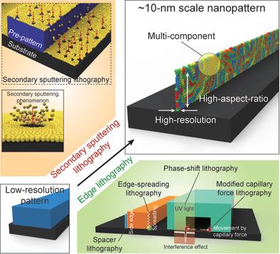
The development of a simple and cost‐effective method for fabricating ≈10 nm scale nanopatterns over large areas is an important issue, owing to the performance enhancement such patterning brings to various applications including sensors, semiconductors, and flexible transparent electrodes. Although nanoimprinting, extreme ultraviolet, electron beams, and scanning probe litho‐graphy are candidates for developing such nanopatterns, they are limited to complicated procedures with low throughput and high startup cost, which are difficult to use in various academic and industry fields. Recently, several easy and cost‐effective lithographic approaches have been reported to produce ≈10 nm scale patterns without defects over large areas. This includes a method of reducing the size using the narrow edge of a pattern, which has been attracting attention for the past several decades. More recently, secondary sputtering lithography using an ion‐bombardment technique was reported as a new method to create high‐resolution and high‐aspect‐ratio structures. Recent progress in simple and cost‐effective top‐down lithography for ≈10 nm scale nanopatterns via edge and secondary sputtering techniques is reviewed. The principles, technical advances, and applications are demonstrated. Finally, the future direction of edge and secondary sputtering lithography research toward issues to be resolved to broaden applications is discussed.
中文翻译:

≈10 nm尺度纳米图案的简单且经济有效的自上而下光刻技术的最新进展:从边缘光刻到二次溅射光刻。
开发一种在大面积上制造≈10nm规模的纳米图案的简单且经济高效的方法是一个重要的问题,由于这种图案的性能得到了提高,从而带给了包括传感器,半导体和柔性透明电极在内的各种应用。尽管纳米压印,极紫外光,电子束和扫描探针平版印刷术是开发此类纳米图案的候选方法,但它们仅限于复杂的过程,低通量和高启动成本,难以在各种学术和工业领域中使用。近来,已经报道了几种简单且具有成本效益的光刻方法,可产生≈10nm规模的图案,而在大面积上没有缺陷。这包括使用图案的窄边减小尺寸的方法,在过去的几十年中一直受到关注。最近,有报道称使用离子轰击技术的二次溅射光刻技术是一种创建高分辨率和高纵横比结构的新方法。本文回顾了通过边缘和二次溅射技术在约10 nm规模的纳米图案上进行简单,经济高效的自顶向下光刻的最新进展。演示了原理,技术进步和应用。最后,讨论了边缘和二次溅射光刻研究的未来方向,以解决要拓宽应用范围的问题。本文回顾了通过边缘和二次溅射技术在约10 nm规模的纳米图案上进行简单,经济高效的自顶向下光刻的最新进展。演示了原理,技术进步和应用。最后,讨论了边缘和二次溅射光刻研究的未来方向,以解决要拓宽应用范围的问题。本文回顾了通过边缘和二次溅射技术在约10 nm规模的纳米图案上进行简单,经济高效的自顶向下光刻的最新进展。演示了原理,技术进步和应用。最后,讨论了边缘和二次溅射光刻研究的未来方向,以解决要拓宽应用范围的问题。
更新日期:2020-04-03
中文翻译:
≈10 nm尺度纳米图案的简单且经济有效的自上而下光刻技术的最新进展:从边缘光刻到二次溅射光刻。
开发一种在大面积上制造≈10nm规模的纳米图案的简单且经济高效的方法是一个重要的问题,由于这种图案的性能得到了提高,从而带给了包括传感器,半导体和柔性透明电极在内的各种应用。尽管纳米压印,极紫外光,电子束和扫描探针平版印刷术是开发此类纳米图案的候选方法,但它们仅限于复杂的过程,低通量和高启动成本,难以在各种学术和工业领域中使用。近来,已经报道了几种简单且具有成本效益的光刻方法,可产生≈10nm规模的图案,而在大面积上没有缺陷。这包括使用图案的窄边减小尺寸的方法,在过去的几十年中一直受到关注。最近,有报道称使用离子轰击技术的二次溅射光刻技术是一种创建高分辨率和高纵横比结构的新方法。本文回顾了通过边缘和二次溅射技术在约10 nm规模的纳米图案上进行简单,经济高效的自顶向下光刻的最新进展。演示了原理,技术进步和应用。最后,讨论了边缘和二次溅射光刻研究的未来方向,以解决要拓宽应用范围的问题。本文回顾了通过边缘和二次溅射技术在约10 nm规模的纳米图案上进行简单,经济高效的自顶向下光刻的最新进展。演示了原理,技术进步和应用。最后,讨论了边缘和二次溅射光刻研究的未来方向,以解决要拓宽应用范围的问题。本文回顾了通过边缘和二次溅射技术在约10 nm规模的纳米图案上进行简单,经济高效的自顶向下光刻的最新进展。演示了原理,技术进步和应用。最后,讨论了边缘和二次溅射光刻研究的未来方向,以解决要拓宽应用范围的问题。


 京公网安备 11010802027423号