Our official English website, www.x-mol.net, welcomes your
feedback! (Note: you will need to create a separate account there.)
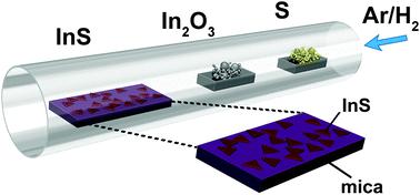
CVD growth of large-area InS atomic layers and device applications.
Nanoscale ( IF 5.8 ) Pub Date : 2020-05-07 , DOI: 10.1039/d0nr01104e Chien-Liang Tu,Kuang-I Lin,Jiang Pu,Tsai-Fu Chung,Chien-Nan Hsiao,An-Ci Huang,Jer-Ren Yang,Taishi Takenobu,Chang-Hsiao Chen
Nanoscale ( IF 5.8 ) Pub Date : 2020-05-07 , DOI: 10.1039/d0nr01104e Chien-Liang Tu,Kuang-I Lin,Jiang Pu,Tsai-Fu Chung,Chien-Nan Hsiao,An-Ci Huang,Jer-Ren Yang,Taishi Takenobu,Chang-Hsiao Chen
|
Group-III monochalcogenides of two-dimensional (2D) layered materials have attracted widespread attention among scientists due to their unique electronic performance and interesting chemical and physical properties. Indium sulfide (InS) is attracting increasing interest from scientists because it has two distinct crystal structures. However, studies on the synthesis of highly crystalline, large-area, and atomically thin-film InS have not been reported thus far. Here, the chemical vapor deposition (CVD) synthesis method of atomic InS crystals has been reported in this paper. The direct chemical vapour phase reaction of metal oxides with chalcogen precursors produces a large-sized hexagonal crystal structure and atomic-thickness InS flakes or films. The InS atomic films are merged with a plurality of triangular InS crystals that are uniform and entire and have surface areas of 1 cm2 and controllable thicknesses in bilayers or trilayers. The properties of the as-grown highly crystalline samples were characterized by spectroscopic and microscopic measurements. The ion-gel gated InS field-effect transistors (FETs) reveal n-type transport behavior, and have an on-off current ratio of >103 and a room-temperature electron mobility of ∼2 cm2 V-1 s-1. Moreover, our CVD InS can be transferred from mica to any substrates, so various 2D materials can be reassembled into vertically stacked heterostructures, thus facilitating the development of heterojunctions and exploration of the properties and applications of their interactions.
中文翻译:

大面积InS原子层的CVD生长及其器件应用。
二维(2D)层状材料的III类单硫族化物因其独特的电子性能以及有趣的化学和物理特性而吸引了科学家的广泛关注。硫化铟(InS)具有两个不同的晶体结构,因此吸引了越来越多的科学家关注。但是,迄今为止,尚未报道有关高结晶,大面积和原子薄膜InS合成的研究。在此,已经报道了原子InS晶体的化学气相沉积(CVD)合成方法。金属氧化物与硫属元素化物前体的直接化学气相反应会产生大尺寸的六方晶体结构和原子厚度的InS薄片或薄膜。InS原子膜与多个均匀且完整的三角形InS晶体融合,并具有1 cm2的表面积和双层或三层厚度可控。生长的高度结晶样品的性质通过光谱和显微镜测量来表征。离子凝胶门控的InS场效应晶体管(FET)表现出n型传输行为,开/关电流比> 103,室温电子迁移率约2 cm2 V-1 s-1。此外,我们的CVD InS可以从云母转移到任何衬底上,因此可以将各种2D材料重新组装成垂直堆叠的异质结构,从而促进异质结的发展以及探索其相互作用的性质和应用。
更新日期:2020-04-03
中文翻译:
大面积InS原子层的CVD生长及其器件应用。
二维(2D)层状材料的III类单硫族化物因其独特的电子性能以及有趣的化学和物理特性而吸引了科学家的广泛关注。硫化铟(InS)具有两个不同的晶体结构,因此吸引了越来越多的科学家关注。但是,迄今为止,尚未报道有关高结晶,大面积和原子薄膜InS合成的研究。在此,已经报道了原子InS晶体的化学气相沉积(CVD)合成方法。金属氧化物与硫属元素化物前体的直接化学气相反应会产生大尺寸的六方晶体结构和原子厚度的InS薄片或薄膜。InS原子膜与多个均匀且完整的三角形InS晶体融合,并具有1 cm2的表面积和双层或三层厚度可控。生长的高度结晶样品的性质通过光谱和显微镜测量来表征。离子凝胶门控的InS场效应晶体管(FET)表现出n型传输行为,开/关电流比> 103,室温电子迁移率约2 cm2 V-1 s-1。此外,我们的CVD InS可以从云母转移到任何衬底上,因此可以将各种2D材料重新组装成垂直堆叠的异质结构,从而促进异质结的发展以及探索其相互作用的性质和应用。


 京公网安备 11010802027423号