Nano Energy ( IF 16.8 ) Pub Date : 2020-04-02 , DOI: 10.1016/j.nanoen.2020.104744 Zhihao Huo , Xiandi Wang , Yufei Zhang , Bensong Wan , Wenqiang Wu , Jianguo Xi , Zheng Yang , Guofeng Hu , Xiangyu Li , Caofeng Pan
|
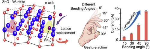
Novel wide-bandgap piezoelectric semiconductor materials, with wurtzite structure, set a great impetus to research, which outreach the promising applications in optoelectronic devices, wearable electronic devices and medical monitoring systems. Here, we studied the piezotronic effect of p-ZnO NW films under strain which were suitable for self-powered tactile sensors. Typically, the doping level was 2 × 1017 cm−3 at the 2% Sb doping in solution. Based on different devices design, it was verified that the piezoelectric charges induced by applied strain could significantly affect the charge carrier separation and transport at the interface/junction. For p-ZnO NW thin film devices, the negative piezoelectric charge reduces Schottky barrier height, while the positive piezoelectric charge increases it. Self-powered strain sensors were then developed based on the changes of piezoelectric potential under different strain, which have a potential candidate for applications in man-machine interaction interface and biomedical sciences.
中文翻译:
用于自供电压电应变传感器的高性能Sb掺杂p-ZnO NW膜
具有纤锌矿结构的新型宽带隙压电半导体材料极大地推动了研究的发展,其在光电子器件,可穿戴电子器件和医疗监控系统中的应用前景广阔。在这里,我们研究了适用于自供电触觉传感器的p-ZnO NW薄膜在应变下的压电效应。通常,掺杂水平为2×10 17 cm -3 在溶液中掺杂2%的Sb。基于不同的器件设计,已验证由施加的应变感应的压电电荷会显着影响界面/结处的电荷载流子分离和传输。对于p-ZnO NW薄膜器件,负压电电荷会降低肖特基势垒高度,而正压电电荷会增加它的高度。然后,根据压电应变在不同应变下的变化,开发了自供电应变传感器,该传感器有潜力在人机交互界面和生物医学领域中得到应用。


 京公网安备 11010802027423号