当前位置:
X-MOL 学术
›
Nano Lett.
›
论文详情
Our official English website, www.x-mol.net, welcomes your
feedback! (Note: you will need to create a separate account there.)
Monolithic Plasmonic Waveguide Architecture for Passive and Active Optical Circuits.
Nano Letters ( IF 9.6 ) Pub Date : 2020-03-31 , DOI: 10.1021/acs.nanolett.9b04612 Charles Chih-Chin Lin 1 , Po-Han Chang 1 , Yiwen Su 1 , Amr S Helmy 1
Nano Letters ( IF 9.6 ) Pub Date : 2020-03-31 , DOI: 10.1021/acs.nanolett.9b04612 Charles Chih-Chin Lin 1 , Po-Han Chang 1 , Yiwen Su 1 , Amr S Helmy 1
Affiliation
|
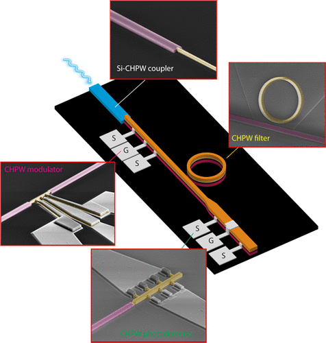
Guided-wave plasmonic circuits are promising platforms for sensing, interconnection, and quantum applications in the subdiffraction regime. Nonetheless, the loss-confinement trade-off remains a collective bottleneck for plasmonic-enhanced optical processes. Here, we report a unique plasmonic waveguide architecture that can alleviate such trade-off and improve the efficiencies of plasmonic-based emission, light-matter-interaction, and detection simultaneously. Specifically, record experimental attributes such as normalized Purcell factor approaching 104, 10 dB amplitude modulation with <1 dB insertion loss and fJ-level switching energy, and photodetection sensitivity and internal quantum efficiency of -54 dBm and 6.4% respectively have been realized within our amorphous-based, coupled-mode plasmonic structure. The ability to support multiple optoelectronic phenomena while providing performance gains over existing plasmonic and dielectric counterparts offers a clear path toward reconfigurable, monolithic plasmonic circuits.
中文翻译:

用于无源和有源光学电路的单片等离子波导架构。
导波等离子体激元电路是用于亚衍射领域中传感,互连和量子应用的有前途的平台。尽管如此,损耗限制的权衡仍然是等离激元增强光学工艺的一个总瓶颈。在这里,我们报告了一种独特的等离激元波导架构,该架构可以减轻这种折衷,并同时提高基于等离激元的发射,光物质相互作用和检测的效率。具体而言,我们已实现了记录的实验属性,例如接近104的归一化Purcell因子,具有<1 dB的插入损耗和fJ级开关能量的10 dB幅度调制,以及分别达到-54 dBm和6.4%的光检测灵敏度和内部量子效率。基于非晶的耦合模式等离子体激元结构。
更新日期:2020-03-31
中文翻译:
用于无源和有源光学电路的单片等离子波导架构。
导波等离子体激元电路是用于亚衍射领域中传感,互连和量子应用的有前途的平台。尽管如此,损耗限制的权衡仍然是等离激元增强光学工艺的一个总瓶颈。在这里,我们报告了一种独特的等离激元波导架构,该架构可以减轻这种折衷,并同时提高基于等离激元的发射,光物质相互作用和检测的效率。具体而言,我们已实现了记录的实验属性,例如接近104的归一化Purcell因子,具有<1 dB的插入损耗和fJ级开关能量的10 dB幅度调制,以及分别达到-54 dBm和6.4%的光检测灵敏度和内部量子效率。基于非晶的耦合模式等离子体激元结构。


 京公网安备 11010802027423号