当前位置:
X-MOL 学术
›
Adv. Mater. Interfaces
›
论文详情
Our official English website, www.x-mol.net, welcomes your feedback! (Note: you will need to create a separate account there.)
Effect of the Degree of the Gate‐Dielectric Surface Roughness on the Performance of Bottom‐Gate Organic Thin‐Film Transistors
Advanced Materials Interfaces ( IF 5.4 ) Pub Date : 2020-03-29 , DOI: 10.1002/admi.201902145 Michael Geiger 1 , Rachana Acharya 1 , Eric Reutter 1 , Thomas Ferschke 2 , Ute Zschieschang 1 , Jürgen Weis 1 , Jens Pflaum 2, 3 , Hagen Klauk 1 , Ralf Thomas Weitz 4, 5
Advanced Materials Interfaces ( IF 5.4 ) Pub Date : 2020-03-29 , DOI: 10.1002/admi.201902145 Michael Geiger 1 , Rachana Acharya 1 , Eric Reutter 1 , Thomas Ferschke 2 , Ute Zschieschang 1 , Jürgen Weis 1 , Jens Pflaum 2, 3 , Hagen Klauk 1 , Ralf Thomas Weitz 4, 5
Affiliation
|
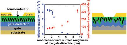
In organic thin‐film transistors (TFTs) fabricated in the inverted (bottom‐gate) device structure, the surface roughness of the gate dielectric onto which the organic‐semiconductor layer is deposited is expected to have a significant effect on the TFT characteristics. To quantitatively evaluate this effect, a method to tune the surface roughness of a gate dielectric consisting of a thin layer of aluminum oxide and an alkylphosphonic acid self‐assembled monolayer over a wide range by controlling a single process parameter, namely the substrate temperature during the deposition of the aluminum gate electrodes, is developed. All other process parameters remain constant in the experiments, so that any differences observed in the TFT performance can be confidently ascribed to effects related to the difference in the gate‐dielectric surface roughness. It is found that an increase in surface roughness leads to a significant decrease in the effective charge‐carrier mobility and an increase in the subthreshold swing. It is shown that a larger gate‐dielectric surface roughness leads to a larger density of grain boundaries in the semiconductor layer, which in turn produces a larger density of localized trap states in the semiconductor.
中文翻译:

栅极介电表面粗糙度的程度对底栅有机薄膜晶体管性能的影响
在倒置(底部栅极)器件结构中制造的有机薄膜晶体管(TFT)中,预期在其上沉积有机半导体层的栅极电介质的表面粗糙度将对TFT特性产生重大影响。为了定量评估这种影响,一种方法是通过控制单个工艺参数(即在加热过程中的基板温度)在很大范围内调节由氧化铝薄层和烷基膦酸自组装单层组成的栅极电介质的表面粗糙度。开发了铝栅电极的沉积。所有其他工艺参数在实验中保持不变,因此,TFT性能中观察到的任何差异都可以确信地归因于与栅介电表面粗糙度差异有关的影响。发现表面粗糙度的增加导致有效电荷载流子迁移率显着降低,并且亚阈值摆幅增加。结果表明,较大的栅介电表面粗糙度会导致半导体层中较大的晶界密度,从而在半导体中产生较大的局部陷阱态密度。
更新日期:2020-03-29
中文翻译:
栅极介电表面粗糙度的程度对底栅有机薄膜晶体管性能的影响
在倒置(底部栅极)器件结构中制造的有机薄膜晶体管(TFT)中,预期在其上沉积有机半导体层的栅极电介质的表面粗糙度将对TFT特性产生重大影响。为了定量评估这种影响,一种方法是通过控制单个工艺参数(即在加热过程中的基板温度)在很大范围内调节由氧化铝薄层和烷基膦酸自组装单层组成的栅极电介质的表面粗糙度。开发了铝栅电极的沉积。所有其他工艺参数在实验中保持不变,因此,TFT性能中观察到的任何差异都可以确信地归因于与栅介电表面粗糙度差异有关的影响。发现表面粗糙度的增加导致有效电荷载流子迁移率显着降低,并且亚阈值摆幅增加。结果表明,较大的栅介电表面粗糙度会导致半导体层中较大的晶界密度,从而在半导体中产生较大的局部陷阱态密度。


 京公网安备 11010802027423号