当前位置:
X-MOL 学术
›
Int. J. Energy Res.
›
论文详情
Our official English website, www.x-mol.net, welcomes your
feedback! (Note: you will need to create a separate account there.)
Structural evolution of chemically deposited binary stacks of Sb2S3‐CuS to phase‐pure CuSbS2 thin films and evaluation of device parameters of CuSbS2/CdS heterojunction
International Journal of Energy Research ( IF 4.3 ) Pub Date : 2020-03-23 , DOI: 10.1002/er.5359 Mou Pal 1 , C. J. Diliegros‐Godines 1 , Goutam K. Gupta 2 , N. R. Mathews 3 , Ambesh Dixit 2
International Journal of Energy Research ( IF 4.3 ) Pub Date : 2020-03-23 , DOI: 10.1002/er.5359 Mou Pal 1 , C. J. Diliegros‐Godines 1 , Goutam K. Gupta 2 , N. R. Mathews 3 , Ambesh Dixit 2
Affiliation
|
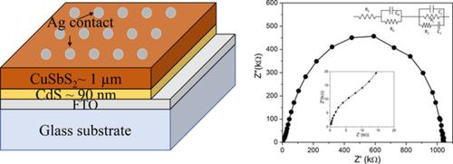
Copper‐based chalcogenide ternary compounds are promising materials to be used as absorber layer in solar cells. In this work, we have reported the preparation of copper antimony sulfide (CAS) thin films by annealing chemically deposited multi‐stack of Sb2S3‐CuS and the effect of thickness ratio between two binary sulfides on the formation of different crystalline phases of Cu‐Sb‐S system. A series of multilayer structure was prepared with different thickness of CuS in order to study the effect of copper concentration on the structural, morphological, optical, and electrical properties of the resulting CuxSb1‐xSy films. The CAS films were characterized by several techniques such as X‐ray diffraction, Raman scattering, UV‐visible spectroscopy, atomic force microscopy, scanning electron microscopy, energy‐dispersive X‐ray spectroscopy, and Hall effect measurements to evaluate their physical properties. The formation of either pure chalcostibite (CuSbS2) or mixed ternary phases containing chalcostibite, famatinite (Cu3SbS4), and tetrahedrite (Cu12Sb4S13) were detected depending on the thickness ratio of Sb2S3 and CuS. Chalcostibite films revealed desired optical and electrical values. Finally, solar cell was fabricated using the heterostructure FTO/CdS/CuSbS2/Ag and characterized by current‐voltage, capacitance‐voltage, and impedance‐spectroscopy measurements achieving a promising ~0.8% efficiency with VOC = 0.484 V, JSC = 5.97 mA/cm2, and FF =27.34%. Impedance measurements revealed a low series resistance in the optimal solar cell, as a result, an increment in open circuit voltage.
中文翻译:

化学沉积的Sb2S3-CuS二元堆叠结构到纯相CuSbS2薄膜的结构演变以及CuSbS2 / CdS异质结的器件参数评估
铜基硫族化物三元化合物是有望用作太阳能电池吸收层的材料。在这项工作中,我们报告了通过化学沉积Sb 2 S 3 -CuS的多叠层退火制备硫化铜锑(CAS)薄膜,以及两种二元硫化物之间的厚度比对形成不同结晶相的影响。 Cu‐Sb‐S系统。为了研究铜浓度对所得Cu x Sb 1-x S y的结构,形态,光学和电学性质的影响,制备了一系列不同厚度的CuS的多层结构。电影。CAS膜通过多种技术进行表征,例如X射线衍射,拉曼散射,紫外可见光谱,原子力显微镜,扫描电子显微镜,能量色散X射线光谱和霍尔效应测量以评估其物理性能。根据Sb 2 S 3的厚度比,检测到纯黄铜矿(CuSbS 2)或含有黄铜矿,辉铁矿(Cu 3 SbS 4)和四面体(Cu 12 Sb 4 S 13)的混合三元相的形成。和CuS。黄铜矿膜显示出所需的光学和电学价值。最后,使用异质结构FTO / CdS / CuSbS 2 / Ag制备太阳能电池,并通过电流-电压,电容-电压和阻抗谱测量表征,在V OC = 0.484 V,J SC = 5.97mA / cm 2,且FF = 27.34%。阻抗测量显示最佳太阳能电池中的串联电阻较低,结果是开路电压增加。
更新日期:2020-03-23
中文翻译:
化学沉积的Sb2S3-CuS二元堆叠结构到纯相CuSbS2薄膜的结构演变以及CuSbS2 / CdS异质结的器件参数评估
铜基硫族化物三元化合物是有望用作太阳能电池吸收层的材料。在这项工作中,我们报告了通过化学沉积Sb 2 S 3 -CuS的多叠层退火制备硫化铜锑(CAS)薄膜,以及两种二元硫化物之间的厚度比对形成不同结晶相的影响。 Cu‐Sb‐S系统。为了研究铜浓度对所得Cu x Sb 1-x S y的结构,形态,光学和电学性质的影响,制备了一系列不同厚度的CuS的多层结构。电影。CAS膜通过多种技术进行表征,例如X射线衍射,拉曼散射,紫外可见光谱,原子力显微镜,扫描电子显微镜,能量色散X射线光谱和霍尔效应测量以评估其物理性能。根据Sb 2 S 3的厚度比,检测到纯黄铜矿(CuSbS 2)或含有黄铜矿,辉铁矿(Cu 3 SbS 4)和四面体(Cu 12 Sb 4 S 13)的混合三元相的形成。和CuS。黄铜矿膜显示出所需的光学和电学价值。最后,使用异质结构FTO / CdS / CuSbS 2 / Ag制备太阳能电池,并通过电流-电压,电容-电压和阻抗谱测量表征,在V OC = 0.484 V,J SC = 5.97mA / cm 2,且FF = 27.34%。阻抗测量显示最佳太阳能电池中的串联电阻较低,结果是开路电压增加。


 京公网安备 11010802027423号