当前位置:
X-MOL 学术
›
Nanoscale Adv.
›
论文详情
Our official English website, www.x-mol.net, welcomes your
feedback! (Note: you will need to create a separate account there.)
On-site growth method of 3D structured multi-layered graphene on silicon nanowires
Nanoscale Advances ( IF 4.6 ) Pub Date : 2020-03-23 , DOI: 10.1039/d0na00098a Steaphan Mark Wallace 1, 2 , Wipakorn Jevasuwan 1 , Naoki Fukata 1, 2
Nanoscale Advances ( IF 4.6 ) Pub Date : 2020-03-23 , DOI: 10.1039/d0na00098a Steaphan Mark Wallace 1, 2 , Wipakorn Jevasuwan 1 , Naoki Fukata 1, 2
Affiliation
|
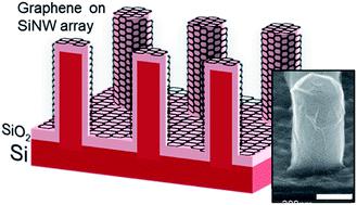
An experimental method is described in which a orderly 3D array of graphene sheets is grown to conform to the shape of an underlying nanowire (NW) substrate that remains on-site. The procedure uses a sacrificial nickel catalyst-based CVD growth process that is capable of producing graphene onto an insulating SiO2 substrate. Nano-imprint silicon NWs serve both as the scaffolding for the catalyst and as the final underlying substrate. The graphene is polycrystalline and multi-layered as expected from this nickel catalyzed growth method. This presents a novel and quick method that can be used to produce conductive graphene sheets in precise shapes and configurations seen in complex device applications but which are difficult to produce with current transfer methods. The geometry of the nanostructured substrate itself contributes to the on-site growth method by making it difficult for the graphene to wash off during wet etching. The SiNWs used in this research have increased surface area and a light trapping effect that, in combination with the graphene, can be used in future sensor and photovoltaic device applications.
中文翻译:

3D结构化多层石墨烯在硅纳米线上的原位生长方法
描述了一种实验方法,其中生长有序的 3D 石墨烯片阵列以符合保留在现场的底层纳米线 (NW) 基板的形状。该过程使用基于牺牲镍催化剂的 CVD 生长工艺,该工艺能够在绝缘的 SiO 2上产生石墨烯基质。纳米压印硅纳米线既可用作催化剂的支架,又可用作最终的底层基板。正如这种镍催化生长方法所预期的那样,石墨烯是多晶的和多层的。这提出了一种新颖且快速的方法,可用于生产复杂器件应用中具有精确形状和配置的导电石墨烯片,但用电流转移方法难以生产。纳米结构基板本身的几何形状通过使石墨烯在湿法蚀刻过程中难以洗掉而有助于原位生长方法。本研究中使用的 SiNW 增加了表面积和光捕获效应,与石墨烯结合,可用于未来的传感器和光伏器件应用。
更新日期:2020-04-24
中文翻译:
3D结构化多层石墨烯在硅纳米线上的原位生长方法
描述了一种实验方法,其中生长有序的 3D 石墨烯片阵列以符合保留在现场的底层纳米线 (NW) 基板的形状。该过程使用基于牺牲镍催化剂的 CVD 生长工艺,该工艺能够在绝缘的 SiO 2上产生石墨烯基质。纳米压印硅纳米线既可用作催化剂的支架,又可用作最终的底层基板。正如这种镍催化生长方法所预期的那样,石墨烯是多晶的和多层的。这提出了一种新颖且快速的方法,可用于生产复杂器件应用中具有精确形状和配置的导电石墨烯片,但用电流转移方法难以生产。纳米结构基板本身的几何形状通过使石墨烯在湿法蚀刻过程中难以洗掉而有助于原位生长方法。本研究中使用的 SiNW 增加了表面积和光捕获效应,与石墨烯结合,可用于未来的传感器和光伏器件应用。


 京公网安备 11010802027423号