当前位置:
X-MOL 学术
›
Diam. Relat. Mater.
›
论文详情
Our official English website, www.x-mol.net, welcomes your
feedback! (Note: you will need to create a separate account there.)
Stable, low-resistance, 1.5 to 3.5 kΩ sq−1, diamond surface conduction with a mixed metal-oxide protective film
Diamond and Related Materials ( IF 4.3 ) Pub Date : 2020-06-01 , DOI: 10.1016/j.diamond.2020.107819 M.W. Geis , J.O. Varghese , M.A. Hollis , Y. Yichen , R.J. Nemanich , C.H. Wuorio , Xi Zhang , G.W. Turner , S.M. Warnock , S.A. Vitale , R.J. Molnar , T. Osadchy , B. Zhang
Diamond and Related Materials ( IF 4.3 ) Pub Date : 2020-06-01 , DOI: 10.1016/j.diamond.2020.107819 M.W. Geis , J.O. Varghese , M.A. Hollis , Y. Yichen , R.J. Nemanich , C.H. Wuorio , Xi Zhang , G.W. Turner , S.M. Warnock , S.A. Vitale , R.J. Molnar , T. Osadchy , B. Zhang
|
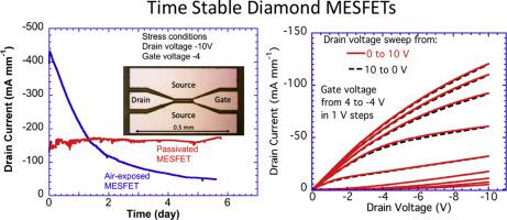
Abstract Semiconducting diamond has the potential for an order-of-magnitude increase in power handling over currently used semiconductors. This is made possible by diamond's higher thermal conductivity and a higher breakdown voltage than any other device-quality semiconductor. Diamond power devices have numerous potential applications in the power grid and in high-power high-frequency RF applications. One approach to leverage diamond's abilities is through the fabrication of field-effect transistors (FETs). The FET is made by forming a p-type surface conductive layer on the diamond surface. This is accomplished by terminating the diamond surface with hydrogen atoms and then coating the surface with a material that contains negative charges to compensate for the positive holes in the p-type layer. Impressive drain current (1.3 A mm−1), maximum operational voltages (>2000 V), and frequencies of unity current gain (fT of 75 GHz) have been demonstrated with this surface conductance method. This surface layer, however, is not stable and FET performance degrades over time on the scale of hours to days. This paper describes an encapsulating layer with a mixed oxide, Al2O3-SiO2, which maintains the resistance of the conductive layer in the range of 1.5 to 3.5 kΩ sq.−1 by protecting the diamond surface while maintaining a stable negative charge.
中文翻译:

稳定、低电阻、1.5 至 3.5 kΩ sq-1、金刚石表面导电,带有混合金属氧化物保护膜
摘要 与目前使用的半导体相比,半导体金刚石有可能使功率处理量增加一个数量级。这是因为金刚石比任何其他器件级半导体具有更高的热导率和更高的击穿电压。金刚石功率器件在电网和大功率高频射频应用中具有众多潜在应用。利用金刚石能力的一种方法是制造场效应晶体管 (FET)。FET是通过在金刚石表面形成p型表面导电层制成的。这是通过用氢原子终止金刚石表面,然后用含有负电荷的材料涂覆表面以补偿 p 型层中的正空穴来实现的。令人印象深刻的漏极电流 (1.3 A mm−1),这种表面电导方法已经证明了最大工作电压 (>2000 V) 和单位电流增益频率 (75 GHz)。然而,该表面层并不稳定,并且 FET 性能会随着时间的推移以数小时到数天的规模下降。本文描述了一种具有混合氧化物 Al2O3-SiO2 的封装层,它通过保护金刚石表面同时保持稳定的负电荷来将导电层的电阻保持在 1.5 到 3.5 kΩ sq.-1 的范围内。
更新日期:2020-06-01
中文翻译:
稳定、低电阻、1.5 至 3.5 kΩ sq-1、金刚石表面导电,带有混合金属氧化物保护膜
摘要 与目前使用的半导体相比,半导体金刚石有可能使功率处理量增加一个数量级。这是因为金刚石比任何其他器件级半导体具有更高的热导率和更高的击穿电压。金刚石功率器件在电网和大功率高频射频应用中具有众多潜在应用。利用金刚石能力的一种方法是制造场效应晶体管 (FET)。FET是通过在金刚石表面形成p型表面导电层制成的。这是通过用氢原子终止金刚石表面,然后用含有负电荷的材料涂覆表面以补偿 p 型层中的正空穴来实现的。令人印象深刻的漏极电流 (1.3 A mm−1),这种表面电导方法已经证明了最大工作电压 (>2000 V) 和单位电流增益频率 (75 GHz)。然而,该表面层并不稳定,并且 FET 性能会随着时间的推移以数小时到数天的规模下降。本文描述了一种具有混合氧化物 Al2O3-SiO2 的封装层,它通过保护金刚石表面同时保持稳定的负电荷来将导电层的电阻保持在 1.5 到 3.5 kΩ sq.-1 的范围内。


 京公网安备 11010802027423号