当前位置:
X-MOL 学术
›
ACS Appl. Electron. Mater.
›
论文详情
Our official English website, www.x-mol.net, welcomes your
feedback! (Note: you will need to create a separate account there.)
Intrinsically Substitutional Carbon Doping in CVD-Grown Monolayer MoS2 and the Band Structure Modulation
ACS Applied Electronic Materials ( IF 4.3 ) Pub Date : 2020-03-20 , DOI: 10.1021/acsaelm.0c00076 Tao Liang 1, 2 , Mohammad Rezwan Habib 1 , Han Xiao 1 , Shuang Xie 3 , Yuhan Kong 2 , Cui Yu 4 , Hideo Iwai 5 , Daisuke Fujita 6 , Nobutaka Hanagata 7 , Hongzheng Chen 2 , Zhihong Feng 4 , Mingsheng Xu 1
ACS Applied Electronic Materials ( IF 4.3 ) Pub Date : 2020-03-20 , DOI: 10.1021/acsaelm.0c00076 Tao Liang 1, 2 , Mohammad Rezwan Habib 1 , Han Xiao 1 , Shuang Xie 3 , Yuhan Kong 2 , Cui Yu 4 , Hideo Iwai 5 , Daisuke Fujita 6 , Nobutaka Hanagata 7 , Hongzheng Chen 2 , Zhihong Feng 4 , Mingsheng Xu 1
Affiliation
|
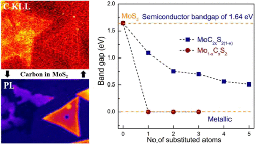
Heterogeneous atom doping has been proven as an efficient route to tune the physical and chemical properties of semiconductors, represented by the technically mature boron and phosphorus doping in bulk silicon. In the two-dimensional (2D) transitional-metal dichalcogenides semiconductors, substitutional doping dominates compared with the interstitial sites doping due to the ultrathin nature of 2D materials. However, unintentional doping can also obscure the structure–property relationship and cause the deviations from the ideally optical/electrical performances. Here, substitutional carbon doping into the monolayer molybdenum disulfide (MoS2) lattice during the normal chemical vapor deposition (CVD) synthesis process is discovered through a thorough analysis of the intermediate and final reaction products. The carbon originates from the relatively low-purity molybdenum precursor, which can be completely eliminated when a high-purity molybdenum precursor is utilized. The carbon-doped monolayer MoS2 exhibits mid-gap states brought by the Mo-d, S-p, and C-p orbital hybridization and gradually reduced band gaps as the doping concentration increases. As a result, the suppressed photoluminescence (PL) intensity and red shift PL position are observed. The finding is fundamental for understanding the unintentional carbon doping process in CVD growth of 2D semiconductors and identifies a source for the inconsistent PL performances in the CVD-derived samples.
中文翻译:

CVD生长单层MoS 2的本征取代碳掺杂和能带结构调制
异质原子掺杂已被证明是调节半导体物理和化学性质的有效途径,以在体硅中技术上成熟的硼和磷掺杂为代表。在二维(2D)过渡金属二硫族半导体中,由于2D材料的超薄特性,与间隙位点掺杂相比,取代掺杂占主导地位。但是,无意的掺杂也会掩盖结构与属性之间的关系,并导致偏离理想的光学/电气性能。在这里,取代碳掺杂到单层二硫化钼(MoS 2通过对中间反应产物和最终反应产物的透彻分析,发现了正常化学气相沉积(CVD)合成过程中的晶格。碳源自相对较低纯度的钼前体,当使用高纯度钼前体时,碳可以完全消除。碳掺杂单层MoS 2表现出Mo- d,S- p和C- p带来的中间能隙状态轨道杂交并随着掺杂浓度的增加逐渐减小带隙。结果,观察到抑制的光致发光(PL)强度和红移PL位置。该发现是理解2D半导体CVD生长中意外碳掺杂过程的基础,并为CVD衍生样品中PL性能不一致的原因提供了依据。
更新日期:2020-03-20
中文翻译:
CVD生长单层MoS 2的本征取代碳掺杂和能带结构调制
异质原子掺杂已被证明是调节半导体物理和化学性质的有效途径,以在体硅中技术上成熟的硼和磷掺杂为代表。在二维(2D)过渡金属二硫族半导体中,由于2D材料的超薄特性,与间隙位点掺杂相比,取代掺杂占主导地位。但是,无意的掺杂也会掩盖结构与属性之间的关系,并导致偏离理想的光学/电气性能。在这里,取代碳掺杂到单层二硫化钼(MoS 2通过对中间反应产物和最终反应产物的透彻分析,发现了正常化学气相沉积(CVD)合成过程中的晶格。碳源自相对较低纯度的钼前体,当使用高纯度钼前体时,碳可以完全消除。碳掺杂单层MoS 2表现出Mo- d,S- p和C- p带来的中间能隙状态轨道杂交并随着掺杂浓度的增加逐渐减小带隙。结果,观察到抑制的光致发光(PL)强度和红移PL位置。该发现是理解2D半导体CVD生长中意外碳掺杂过程的基础,并为CVD衍生样品中PL性能不一致的原因提供了依据。


 京公网安备 11010802027423号