当前位置:
X-MOL 学术
›
Int. J. Energy Res.
›
论文详情
Our official English website, www.x-mol.net, welcomes your
feedback! (Note: you will need to create a separate account there.)
Simulation studies on photovoltaic response of ultrathin CuSb(S/Se)2 ternary compound semiconductors absorber‐based single junction solar cells
International Journal of Energy Research ( IF 4.3 ) Pub Date : 2020-01-21 , DOI: 10.1002/er.5158 Goutam Kumar Gupta 1, 2 , Ambesh Dixit 1
International Journal of Energy Research ( IF 4.3 ) Pub Date : 2020-01-21 , DOI: 10.1002/er.5158 Goutam Kumar Gupta 1, 2 , Ambesh Dixit 1
Affiliation
|
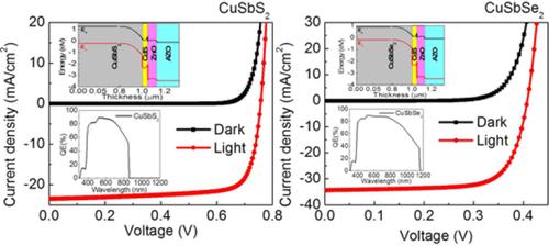
Copper‐based ternary CuSb(S/Se)2 compound semiconductors are showing promise for ultrathin photovoltaic devices. The high absorption coefficient of these semiconductors makes them suitable for very thin absorber, where maximum absorption can be achieved in a photovoltaic device with only nanometers thick CuSb(S/Se)2 based thin films. The device structure under consideration consists of AZO/i‐ZnO/n‐CdS/absorber layer/back contact, as the constituent material layers. The device structure is simulated using one dimensional solar cell capacitance simulator (SCAPS 1D) under one sun illumination and considering flat band approximation for the back contact and CuSb(S/Se)2 interface. The optimized single junction device efficiencies are approximately 14% and approximately 10.18% with CuSbS2 and CuSbSe2 absorbers, respectively. Further, the impact of various material parameters such as thickness, acceptor concentration of bulk absorber layer, donor concentration of CdS buffer layer, and defects present at bulk absorber layer and at the buffer/absorber interface is discussed in correlation with the photovoltaic performance of the considered devices. The bandgap of CuSb(S/Se)2 reduces linearly with Se alloying, and their impact on device performance is quantified in terms of capacitance voltage (CV), capacitance frequency (Cf), and impedance spectra of the photovoltaic device.
中文翻译:

基于超薄CuSb(S / Se)2三元化合物半导体吸收体的单结太阳能电池光伏响应的仿真研究
铜基三元CuSb(S / Se)2化合物半导体显示出超薄光伏器件的前景。这些半导体的高吸收系数使它们适合于非常薄的吸收体,在这种吸收体中,仅基于纳米厚的CuSb(S / Se)2薄膜的光伏器件就可以实现最大吸收。所考虑的器件结构由AZO / i-ZnO / n-CdS /吸收层/背面触点组成,构成材料层。使用一维太阳能电池电容模拟器(SCAPS 1D)在一个阳光照射下并考虑背接触和CuSb(S / Se)2的平坦带近似来模拟器件结构接口。使用CuSbS 2和CuSbSe 2吸收剂时,优化的单结器件效率分别约为14%和10.18%。此外,讨论了各种材料参数的影响,例如厚度,本体吸收层的受体浓度,CdS缓冲层的施主浓度以及本体吸收层和缓冲/吸收体界面处存在的缺陷,并与光电性能相关。被认为是设备。CuSb(S / Se)2的带隙随Se合金化而线性减小,并且根据光伏器件的电容电压(CV),电容频率(Cf)和阻抗谱来量化其对器件性能的影响。
更新日期:2020-01-21
中文翻译:
基于超薄CuSb(S / Se)2三元化合物半导体吸收体的单结太阳能电池光伏响应的仿真研究
铜基三元CuSb(S / Se)2化合物半导体显示出超薄光伏器件的前景。这些半导体的高吸收系数使它们适合于非常薄的吸收体,在这种吸收体中,仅基于纳米厚的CuSb(S / Se)2薄膜的光伏器件就可以实现最大吸收。所考虑的器件结构由AZO / i-ZnO / n-CdS /吸收层/背面触点组成,构成材料层。使用一维太阳能电池电容模拟器(SCAPS 1D)在一个阳光照射下并考虑背接触和CuSb(S / Se)2的平坦带近似来模拟器件结构接口。使用CuSbS 2和CuSbSe 2吸收剂时,优化的单结器件效率分别约为14%和10.18%。此外,讨论了各种材料参数的影响,例如厚度,本体吸收层的受体浓度,CdS缓冲层的施主浓度以及本体吸收层和缓冲/吸收体界面处存在的缺陷,并与光电性能相关。被认为是设备。CuSb(S / Se)2的带隙随Se合金化而线性减小,并且根据光伏器件的电容电压(CV),电容频率(Cf)和阻抗谱来量化其对器件性能的影响。


 京公网安备 11010802027423号