当前位置:
X-MOL 学术
›
ACS Appl. Mater. Interfaces
›
论文详情
Our official English website, www.x-mol.net, welcomes your feedback! (Note: you will need to create a separate account there.)
Tunable 1/f Noise in CVD Bernal-Stacked Bilayer Graphene Transistors
ACS Applied Materials & Interfaces ( IF 9.5 ) Pub Date : 2020-04-02 , DOI: 10.1021/acsami.9b21070 Mengchuan Tian 1 , Qianlan Hu 1 , Chengru Gu 1 , Xiong Xiong 1 , Zhenfeng Zhang 1 , Xuefei Li 1 , Yanqing Wu 1, 2, 3
ACS Applied Materials & Interfaces ( IF 9.5 ) Pub Date : 2020-04-02 , DOI: 10.1021/acsami.9b21070 Mengchuan Tian 1 , Qianlan Hu 1 , Chengru Gu 1 , Xiong Xiong 1 , Zhenfeng Zhang 1 , Xuefei Li 1 , Yanqing Wu 1, 2, 3
Affiliation
|
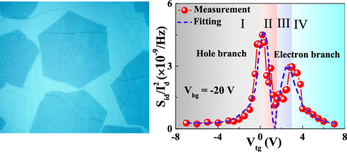
Low-frequency noise is a key performance-limiting factor in almost all electronic systems. Thanks to its excellent characteristics such as exceptionally high electron mobility, graphene has high potential for future low-noise electronic applications. Here, we present an experimental analysis of low-frequency noise in dual-gate graphene transistors based on chemical vapor-deposited Bernal-stacked bilayer graphene. The fabricated dual-gate bilayer graphene transistors adopt atomic layer-deposited Al2O3 and HfSiO as top-gate and back-gate dielectric, respectively. Our results reveal an obvious M-shape gate-dependent noise behavior which can be well described by a quantitative charge-noise model. The minimal area normalized noise spectral density at 10 Hz reaches as low as about 3 × 10⁻¹⁰ μm2·Hz–1 at room temperature, much lower than the best results reported previously for graphene devices. In addition, the observed noise level further decreases by more than 10 times at temperature of 20 K. Meanwhile, the noise spectral density amplitude can be tuned by more than 2 orders of magnitude at 20 K by dual-gate voltages.
中文翻译:

CVD Bernal堆叠双层石墨烯晶体管中的可调1 / f噪声
在几乎所有电子系统中,低频噪声都是关键的性能限制因素。由于其出色的特性(例如,极高的电子迁移率),石墨烯在未来的低噪声电子应用中具有巨大潜力。在这里,我们介绍了基于化学气相沉积贝尔纳堆叠双层石墨烯的双栅石墨烯晶体管中的低频噪声的实验分析。所制造的双栅双层石墨烯晶体管分别采用沉积有原子层的Al 2 O 3和HfSiO作为顶栅和背栅电介质。我们的结果揭示了明显的M型门相关噪声行为,可以通过定量电荷噪声模型很好地描述它。10 Hz时的最小面积归一化噪声频谱密度可低至约3×10⁻¹⁰微米2 ·赫兹-1在室温下,远低于最佳的结果先前对石墨烯器件的报道。此外,在20 K的温度下,观察到的噪声水平进一步降低了10倍以上。同时,通过双栅极电压,在20 K时可以将噪声频谱密度幅度调整超过2个数量级。
更新日期:2020-04-03
中文翻译:
CVD Bernal堆叠双层石墨烯晶体管中的可调1 / f噪声
在几乎所有电子系统中,低频噪声都是关键的性能限制因素。由于其出色的特性(例如,极高的电子迁移率),石墨烯在未来的低噪声电子应用中具有巨大潜力。在这里,我们介绍了基于化学气相沉积贝尔纳堆叠双层石墨烯的双栅石墨烯晶体管中的低频噪声的实验分析。所制造的双栅双层石墨烯晶体管分别采用沉积有原子层的Al 2 O 3和HfSiO作为顶栅和背栅电介质。我们的结果揭示了明显的M型门相关噪声行为,可以通过定量电荷噪声模型很好地描述它。10 Hz时的最小面积归一化噪声频谱密度可低至约3×10⁻¹⁰微米2 ·赫兹-1在室温下,远低于最佳的结果先前对石墨烯器件的报道。此外,在20 K的温度下,观察到的噪声水平进一步降低了10倍以上。同时,通过双栅极电压,在20 K时可以将噪声频谱密度幅度调整超过2个数量级。


 京公网安备 11010802027423号