Our official English website, www.x-mol.net, welcomes your
feedback! (Note: you will need to create a separate account there.)
Lab-on-fiber: plasmonic nano-arrays for sensing
Nanoscale ( IF 5.8 ) Pub Date : 2020/03/17 , DOI: 10.1039/d0nr00040j Qi Wang 1, 2, 3, 4, 5 , Lei Wang 1, 2, 3, 4
Nanoscale ( IF 5.8 ) Pub Date : 2020/03/17 , DOI: 10.1039/d0nr00040j Qi Wang 1, 2, 3, 4, 5 , Lei Wang 1, 2, 3, 4
Affiliation
|
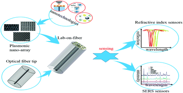
For sensors based on the electromagnetic resonance whether the surface plasmon resonance (SPR) or localized surface plasmon resonance (LSPR), enhancing the light–matter interactions is the most critical and important way to improve their performance. Plasmonic nano-arrays are a kind of periodic metal or dielectric nanostructure formed by nanofabrication technology and can effectively enhance the light–matter interactions by tuning structural parameters to cause different optical effects due to their ultra-high degree of freedom. At the same time, a plug-and-play, remote microsensor suitable for limited environments (such as in vivo systems) may be realized due to the rise of lab-on-fiber technology and the progress of nanofabrication technology for unconventional substrates (such as an optical fiber tip). In this paper, the advantages and disadvantages of different nanofabrication technologies are briefly introduced and compared firstly, and then the applications of optical fiber sensors (OFS) based on different plasmonic nano-arrays are reviewed. Plasmonic nano-array OFS are divided into two categories: refractive index sensors based on the sensitivity of the array to the surrounding environment and surface enhanced Raman scattering (SERS) sensors based on the enhancement ability of the local electric field around the array. In this review, the present sensors are compared and analyzed from the aspects of the geometry, material and dimensions of plasmonic nano-arrays and the main research directions and progress are summarized. Finally, the future development trend is proposed.
中文翻译:

光纤实验室:用于传感的等离激元纳米阵列
对于基于电磁共振的传感器,无论是表面等离子体激元共振(SPR)还是局部表面等离子体激元共振(LSPR),增强光-质相互作用都是提高其性能的最关键也是最重要的方法。等离子体纳米阵列是通过纳米制造技术形成的一种周期性金属或介电纳米结构,由于其超高自由度,可以通过调节结构参数以引起不同的光学效应,从而有效地增强光-物质相互作用。同时,即插即用的远程微传感器适用于有限的环境(例如体内光纤实验室技术的兴起和非常规基材(例如光纤尖端)的纳米加工技术的进步,可以实现这些系统。本文首先简要介绍并比较了不同纳米制造技术的优缺点,然后综述了基于不同等离激元纳米阵列的光纤传感器的应用。等离子体纳米阵列OFS分为两类:基于阵列对周围环境敏感度的折射率传感器和基于阵列周围局部电场增强能力的表面增强拉曼散射(SERS)传感器。在这篇评论中,从几何学方面对当前传感器进行了比较和分析,概述了等离子体纳米阵列的材料和尺寸以及主要的研究方向和进展。最后,提出了未来的发展趋势。
更新日期:2020-04-09
中文翻译:
光纤实验室:用于传感的等离激元纳米阵列
对于基于电磁共振的传感器,无论是表面等离子体激元共振(SPR)还是局部表面等离子体激元共振(LSPR),增强光-质相互作用都是提高其性能的最关键也是最重要的方法。等离子体纳米阵列是通过纳米制造技术形成的一种周期性金属或介电纳米结构,由于其超高自由度,可以通过调节结构参数以引起不同的光学效应,从而有效地增强光-物质相互作用。同时,即插即用的远程微传感器适用于有限的环境(例如体内光纤实验室技术的兴起和非常规基材(例如光纤尖端)的纳米加工技术的进步,可以实现这些系统。本文首先简要介绍并比较了不同纳米制造技术的优缺点,然后综述了基于不同等离激元纳米阵列的光纤传感器的应用。等离子体纳米阵列OFS分为两类:基于阵列对周围环境敏感度的折射率传感器和基于阵列周围局部电场增强能力的表面增强拉曼散射(SERS)传感器。在这篇评论中,从几何学方面对当前传感器进行了比较和分析,概述了等离子体纳米阵列的材料和尺寸以及主要的研究方向和进展。最后,提出了未来的发展趋势。


 京公网安备 11010802027423号