当前位置:
X-MOL 学术
›
Mater. Horiz.
›
论文详情
Our official English website, www.x-mol.net, welcomes your
feedback! (Note: you will need to create a separate account there.)
Strain engineering coupled with optical regulation towards a high-sensitivity In2S3 photodetector
Materials Horizons ( IF 12.2 ) Pub Date : 2020-03-13 , DOI: 10.1039/d0mh00243g Jianting Lu 1, 2, 3 , Jiandong Yao 2, 4, 5, 6, 7 , Jiahao Yan 2, 3, 8, 9 , Wei Gao 1, 2, 3 , Le Huang 1, 2, 3 , Zhaoqiang Zheng 1, 2, 3, 10, 11 , Menglong Zhang 2, 3, 12, 13 , Jingbo Li 2, 3, 12, 13, 14
Materials Horizons ( IF 12.2 ) Pub Date : 2020-03-13 , DOI: 10.1039/d0mh00243g Jianting Lu 1, 2, 3 , Jiandong Yao 2, 4, 5, 6, 7 , Jiahao Yan 2, 3, 8, 9 , Wei Gao 1, 2, 3 , Le Huang 1, 2, 3 , Zhaoqiang Zheng 1, 2, 3, 10, 11 , Menglong Zhang 2, 3, 12, 13 , Jingbo Li 2, 3, 12, 13, 14
Affiliation
|
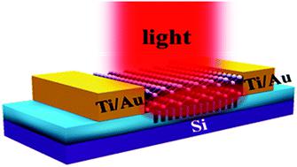
Non-layered 2D materials exhibit intriguing properties, widening the scope of 2D libraries and promising considerable potential for applications in next-generation optoelectronics. However, due to their surface dangling bonds and weak light adsorption arising from their atomically thin thickness, their photosensitivity is still limited. Herein, we achieve an ultrasensitive 2D In2S3 photodetector by adopting strain engineering coupled with optical regulation. A SiO2 nanograting array was introduced to construct a strained morphology of 2D In2S3. This morphology induces charge localization and renders a back-to-back built-in electric field array, which efficiently suppresses the dark current and separates the photo-excited carriers. Simultaneously, the SiO2 nanograting array realizes light management and improves its light harvesting. As a result, the device presents an ultralow dark current of 3.2 pA with a high signal-to-noise ratio of up to 1.7 × 10⁶. In particular, a prominent photoresponsivity of 1810 A W−1, an excellent detectivity of 2.09 × 10¹⁵ Jones and a fast response speed of 0.41 ms are achieved. This work depicts an effective scheme to associate photonic/electronic property manipulation for optoelectronic applications.
中文翻译:

应变工程与针对高灵敏度In2S3光电探测器的光学调节相结合
非分层2D材料具有吸引人的特性,拓宽了2D库的范围,并有望在下一代光电子学中应用。但是,由于它们的表面悬挂键和由于原子薄的厚度而引起的弱光吸收,它们的光敏性仍然受到限制。在这里,我们通过采用应变工程与光学调节相结合,实现了超灵敏的2D In 2 S 3光电探测器。引入SiO 2纳米光栅阵列以构建2D In 2 S 3的应变形态。这种形态引起电荷局部化,并形成了背靠背的内置电场阵列,该阵列有效地抑制了暗电流并分离了光激发载流子。同时,SiO 2纳米光栅阵列实现了光管理并改善了光收集。结果,该器件呈现出3.2 pA的超低暗电流和高达1.7×10 6的高信噪比。尤其是,实现了1810 AW -1的出色光响应性,2.09×10 15 Jones的出色检测率和0.41 ms的快速响应速度。这项工作描绘了一种有效的方案,将光子/电子属性操纵与光电应用相关联。
更新日期:2020-03-13
中文翻译:
应变工程与针对高灵敏度In2S3光电探测器的光学调节相结合
非分层2D材料具有吸引人的特性,拓宽了2D库的范围,并有望在下一代光电子学中应用。但是,由于它们的表面悬挂键和由于原子薄的厚度而引起的弱光吸收,它们的光敏性仍然受到限制。在这里,我们通过采用应变工程与光学调节相结合,实现了超灵敏的2D In 2 S 3光电探测器。引入SiO 2纳米光栅阵列以构建2D In 2 S 3的应变形态。这种形态引起电荷局部化,并形成了背靠背的内置电场阵列,该阵列有效地抑制了暗电流并分离了光激发载流子。同时,SiO 2纳米光栅阵列实现了光管理并改善了光收集。结果,该器件呈现出3.2 pA的超低暗电流和高达1.7×10 6的高信噪比。尤其是,实现了1810 AW -1的出色光响应性,2.09×10 15 Jones的出色检测率和0.41 ms的快速响应速度。这项工作描绘了一种有效的方案,将光子/电子属性操纵与光电应用相关联。


 京公网安备 11010802027423号