Our official English website, www.x-mol.net, welcomes your
feedback! (Note: you will need to create a separate account there.)
Air-stable N-type printed carbon nanotube thin film transistors for CMOS logic circuits
Carbon ( IF 10.5 ) Pub Date : 2020-08-01 , DOI: 10.1016/j.carbon.2020.03.012 Miaomiao Wei , Malo Robin , Luis Portilla , Yunfei Ren , Shuangshuang Shao , Lan Bai , Yu Cao , Vincenzo Pecunia , Zheng Cui , Jianwen Zhao
Carbon ( IF 10.5 ) Pub Date : 2020-08-01 , DOI: 10.1016/j.carbon.2020.03.012 Miaomiao Wei , Malo Robin , Luis Portilla , Yunfei Ren , Shuangshuang Shao , Lan Bai , Yu Cao , Vincenzo Pecunia , Zheng Cui , Jianwen Zhao
|
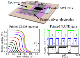
Abstract The lack of long-term air-stable and solution-processed n-doping methods for printed single-walled carbon nanotube (SWCNT) thin film transistors (TFTs) limits their integrations into printed complementary metal-oxide-semiconductor (CMOS) circuits. In this paper, a new chemically modified epoxy amine ink was developed as the chemical dopant and encapsulant to enable the uniform n-type SWCNT-TFTs with long-term air stability (6 months). The epoxy amine inks were dropped onto the printed p-type TFT device channels in a single-step solution process. As a result, printed top-contact n-type SWCNT-TFTs were obtained with well-balanced electrical chararcteristics comparable to their p-type counterparts. The matched p-type and n-type SWCNT-TFTs were thus integrated into the printed CMOS inverters and NAND gates, which have both achieved proper logic operation at supply voltages below 1 V. In particular, the CMOS inverters could operate with VDD down to 0.3V with associated peak power consumption of 0.06 μW, showing full rail-to-rail output swings with voltage gains up to 22, trip voltages of ∼VDD/2, and maximum noise margin of 0.42 V at VDD = 1.1 V (∼76.4% of VDD/2). Furthermore, the static characteristics of CMOS inverters could be maintained for 3 months with negligible changes, proving the feasibility of this long-term air-stable n-doping method.
中文翻译:

用于CMOS逻辑电路的空气稳定N型印刷碳纳米管薄膜晶体管
摘要 印刷单壁碳纳米管 (SWCNT) 薄膜晶体管 (TFT) 缺乏长期空气稳定和溶液处理的 n 掺杂方法,限制了它们与印刷互补金属氧化物半导体 (CMOS) 电路的集成。在本文中,开发了一种新的化学改性环氧胺油墨作为化学掺杂剂和封装剂,使均匀的 n 型 SWCNT-TFT 具有长期空气稳定性(6 个月)。在一步溶液过程中,环氧胺油墨滴在印刷的 p 型 TFT 器件通道上。结果,印刷的顶部接触 n 型 SWCNT-TFT 具有与 p 型对应物相当的平衡良好的电特性。因此,匹配的 p 型和 n 型 SWCNT-TFT 被集成到印刷 CMOS 反相器和与非门中,两者都在低于 1 V 的电源电压下实现了正确的逻辑操作。 特别是,CMOS 反相器可以在 VDD 低至 0.3V 的情况下工作,相关峰值功耗为 0.06 μW,显示完整的轨到轨输出摆幅,电压增益升高到 22,跳变电压为 ~VDD/2,在 VDD = 1.1 V(VDD/2 的 ~76.4%)时最大噪声容限为 0.42 V。此外,CMOS反相器的静态特性可以保持3个月而变化可以忽略不计,证明了这种长期空气稳定n掺杂方法的可行性。4% 的 VDD/2)。此外,CMOS反相器的静态特性可以保持3个月而变化可以忽略不计,证明了这种长期空气稳定n掺杂方法的可行性。4% 的 VDD/2)。此外,CMOS反相器的静态特性可以保持3个月而变化可以忽略不计,证明了这种长期空气稳定n掺杂方法的可行性。
更新日期:2020-08-01
中文翻译:
用于CMOS逻辑电路的空气稳定N型印刷碳纳米管薄膜晶体管
摘要 印刷单壁碳纳米管 (SWCNT) 薄膜晶体管 (TFT) 缺乏长期空气稳定和溶液处理的 n 掺杂方法,限制了它们与印刷互补金属氧化物半导体 (CMOS) 电路的集成。在本文中,开发了一种新的化学改性环氧胺油墨作为化学掺杂剂和封装剂,使均匀的 n 型 SWCNT-TFT 具有长期空气稳定性(6 个月)。在一步溶液过程中,环氧胺油墨滴在印刷的 p 型 TFT 器件通道上。结果,印刷的顶部接触 n 型 SWCNT-TFT 具有与 p 型对应物相当的平衡良好的电特性。因此,匹配的 p 型和 n 型 SWCNT-TFT 被集成到印刷 CMOS 反相器和与非门中,两者都在低于 1 V 的电源电压下实现了正确的逻辑操作。 特别是,CMOS 反相器可以在 VDD 低至 0.3V 的情况下工作,相关峰值功耗为 0.06 μW,显示完整的轨到轨输出摆幅,电压增益升高到 22,跳变电压为 ~VDD/2,在 VDD = 1.1 V(VDD/2 的 ~76.4%)时最大噪声容限为 0.42 V。此外,CMOS反相器的静态特性可以保持3个月而变化可以忽略不计,证明了这种长期空气稳定n掺杂方法的可行性。4% 的 VDD/2)。此外,CMOS反相器的静态特性可以保持3个月而变化可以忽略不计,证明了这种长期空气稳定n掺杂方法的可行性。4% 的 VDD/2)。此外,CMOS反相器的静态特性可以保持3个月而变化可以忽略不计,证明了这种长期空气稳定n掺杂方法的可行性。


 京公网安备 11010802027423号