当前位置:
X-MOL 学术
›
ACS Appl. Electron. Mater.
›
论文详情
Our official English website, www.x-mol.net, welcomes your feedback! (Note: you will need to create a separate account there.)
Facile p-Doping of Few-Layer MoTe2 by Controllable Surface Oxidation toward High-Performance Complementary Devices
ACS Applied Electronic Materials ( IF 4.7 ) Pub Date : 2020-03-08 , DOI: 10.1021/acsaelm.9b00848 Yuxuan Ke 1 , Dianyu Qi 1 , Cheng Han 1 , Jidong Liu 1 , Jiaqi Zhu 1 , Yuanjiang Xiang 1 , Wenjing Zhang 1
ACS Applied Electronic Materials ( IF 4.7 ) Pub Date : 2020-03-08 , DOI: 10.1021/acsaelm.9b00848 Yuxuan Ke 1 , Dianyu Qi 1 , Cheng Han 1 , Jidong Liu 1 , Jiaqi Zhu 1 , Yuanjiang Xiang 1 , Wenjing Zhang 1
Affiliation
|
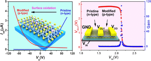
High-performance field-effect transistors based on two-dimensional (2D) semiconductors have been realized, but they often exhibit inherent transport property. Local p- and n-doping on same the semiconductor is essential for realizing the basic components of integrated circuits, such as diodes and logic inverters. However, existing doping technologies on 2D semiconductors are complex or expensive. Here, a simple and low-cost method for p-doping of few-layer MoTe2 transistor is demonstrated. Air heating at a low temperature of 100 °C induces a continuous and efficient modulation of carrier polarity from n- to p-type, and the doping effect can be controlled by adjusting the heating time. The hole mobility of MoTe2 is significantly enhanced from 0.3 to 25.8 cm2 V–1 s–1 by 2 orders of magnitude. The doping effect originates from the surface oxidation of few-layer MoTe2. Based on the method, MoTe2-based logic devices were fabricated, realizing p–n diode with an ideality factor of 1.3 and rectification ratio of ∼3 × 10³ and complementary inverters with a high gain of ∼108. The facile method shows great potential for developing high-performance electronic devices with 2D semiconductors.
中文翻译:

通过向高性能互补器件的可控表面氧化,可以轻松地对少量MoTe 2进行p掺杂。
已经实现了基于二维(2D)半导体的高性能场效应晶体管,但是它们通常表现出固有的传输特性。在同一半导体上进行局部p和n掺杂对于实现集成电路的基本组件(如二极管和逻辑反相器)至关重要。但是,现有的2D半导体掺杂技术既复杂又昂贵。在此,说明了一种简单且低成本的用于p掺杂几层MoTe 2晶体管的方法。在100°C的低温下进行空气加热会引起载流子极性从n型到p型的连续有效调制,并且可以通过调整加热时间来控制掺杂效果。MoTe 2的空穴迁移率从0.3提高到25.8 cm 2 V–1 s –1 2个数量级。掺杂效应源自多层MoTe 2的表面氧化。基于该方法,制造了基于MoTe 2的逻辑器件,实现了理想因数为1.3,整流比为〜3×10 3的p-n二极管以及高增益为〜108的互补反相器。简便的方法显示出开发具有2D半导体的高性能电子设备的巨大潜力。
更新日期:2020-03-08
中文翻译:
通过向高性能互补器件的可控表面氧化,可以轻松地对少量MoTe 2进行p掺杂。
已经实现了基于二维(2D)半导体的高性能场效应晶体管,但是它们通常表现出固有的传输特性。在同一半导体上进行局部p和n掺杂对于实现集成电路的基本组件(如二极管和逻辑反相器)至关重要。但是,现有的2D半导体掺杂技术既复杂又昂贵。在此,说明了一种简单且低成本的用于p掺杂几层MoTe 2晶体管的方法。在100°C的低温下进行空气加热会引起载流子极性从n型到p型的连续有效调制,并且可以通过调整加热时间来控制掺杂效果。MoTe 2的空穴迁移率从0.3提高到25.8 cm 2 V–1 s –1 2个数量级。掺杂效应源自多层MoTe 2的表面氧化。基于该方法,制造了基于MoTe 2的逻辑器件,实现了理想因数为1.3,整流比为〜3×10 3的p-n二极管以及高增益为〜108的互补反相器。简便的方法显示出开发具有2D半导体的高性能电子设备的巨大潜力。


 京公网安备 11010802027423号